Successive Approximation Register Analog to Digital Converter (SAR ADC or A/D)
Intro:SAR is frequently used for medium-to-high-resolution applications with sample rates under 5 Msps.The SAR architecture allows for high-performance, low-power ADCs to be packaged in small form factors for today’s demanding applications.
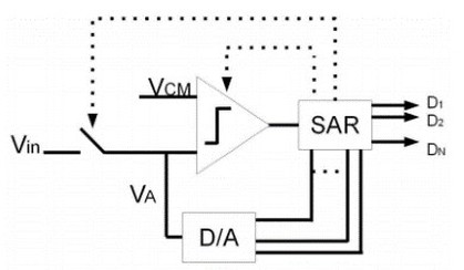
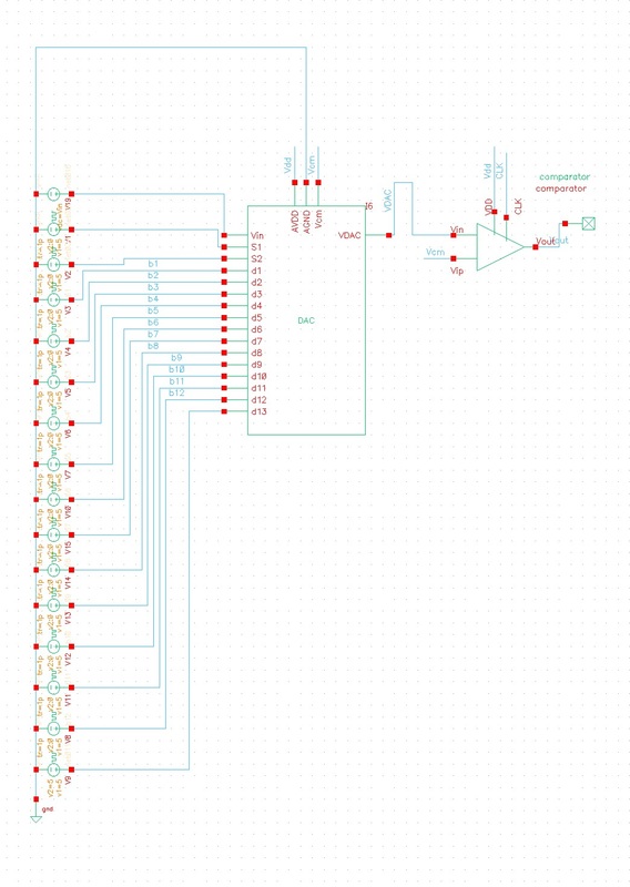
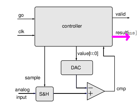
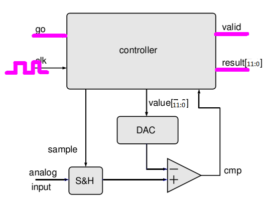
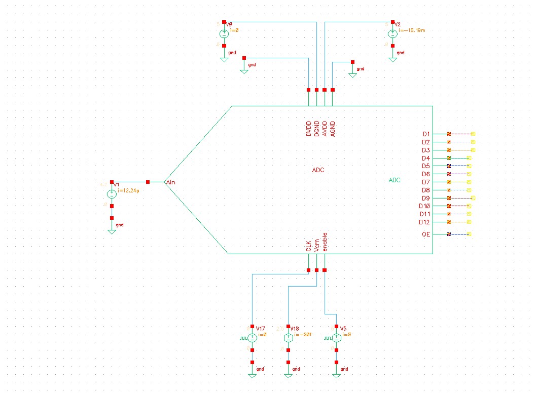
Basic Concept:A SAR ADC uses a successive test algorithm to determine the voltage at an input node. As seen in the figure to the right, this includes a Digital to Analog converter(DAC). The DAC generates a reference voltage for a comparator which will test whether the input voltage is higher or lower than the voltage at the output of the DAC. The output of the comparator determines the next digital output of the SAR ADC iteration cycle. This process repeats until all the bits in the 12-bit value corresponding to the voltage that is sent to the DAC are set.
|
|
The Digital to Analog Converter
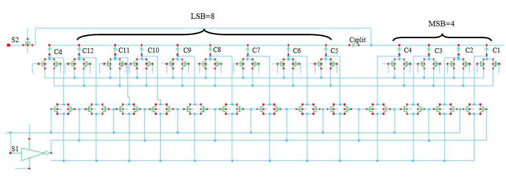
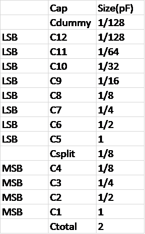
The DAC design method we used in this project was a capacitive string DAC.
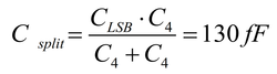
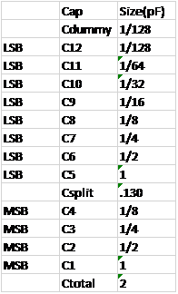
To the right is the table of capacitors used in the DAC with their corresponding size. The capacitor array is split into Most significant bits and Least significant bits to maximize the size of the LSB capacitors. We did not design it to be a single array because that would require very small capacitors which would be difficult to fabricate. This division is done by adding a capacitor in series with the parallel capacitors which is denoted as Csplit in the table. The value of the split capacitor is determined by the series capacitor equation as shown to the right. The schematic of the C-DAC is below: |
|
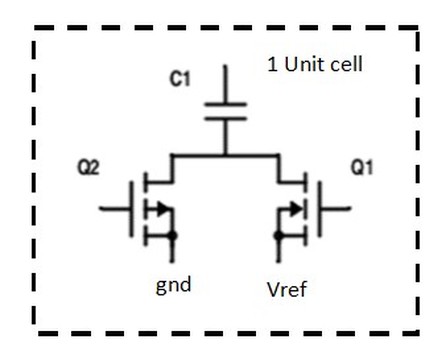
DAC Switch Sizing
|
To meet the rise time and fall time requirement for the capacitors in the DAC, we needed to size the switches for the capacitors accordingly. To do this, we made a unit cell which is a fixed size and made a number of copies of this cell for each capacitor so the circuit would have the same settling time for each capacitor. The requirement for the project was to have a 100K samples per second, so we need a settling time of at most 10 microseconds. From this, we can calculate the charging and discharging transistor channel resistance required to achieve the sample rate desired.
|
DAC output before sizing switches
|

DAC output after sizing switches
|
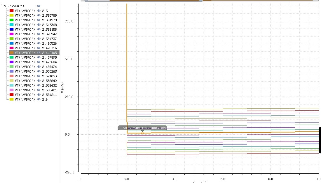
Vcm Sweep Simulation
|
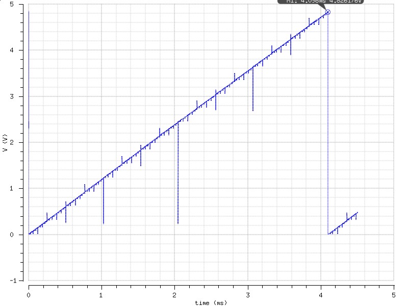
As we can see, before we size the switches, in the figure to the left above, there were multiple glitches occurring on the line. But after we sized our switches, the glitches were reduced effectively. We were confused why the DAC only measured 4.8V instead of our expected 5V. Another problem needing to be mentioned here is that there is an offset on the DAC. We reduced the offset temporarily by finding a good common mode voltage Vcm for DAC. We set Vcm as variable and swept the voltage and plotted it in the figure to the left.
As you can see, the best Voffset occurs when Vcm is 2.44V, at which we have the smallest offset of 9.18mV. But changing V to adjust the offset is not the best way to eliminate offset. Instead, we chose to use offset cancellation to cancel the offset. The offset cancellation is discussed in the Comparator section later on this page. |
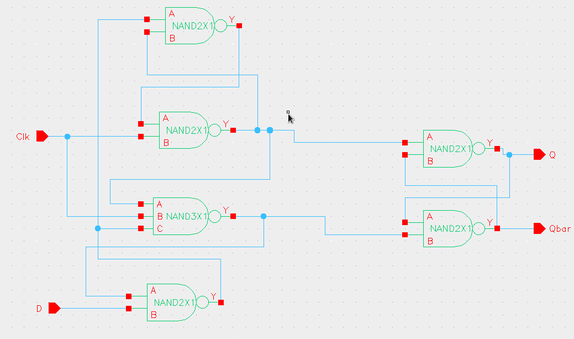
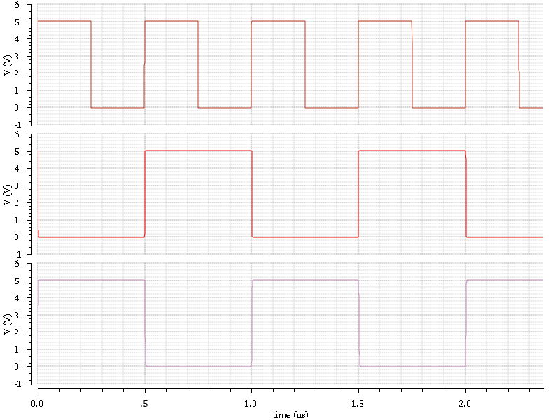
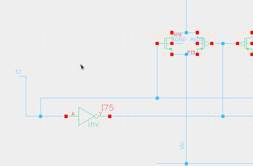
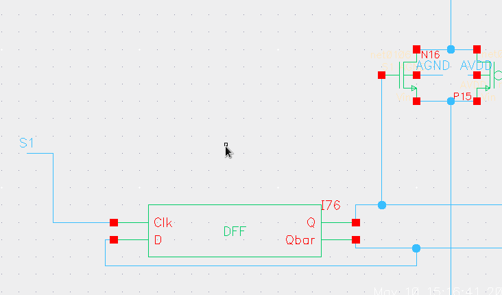
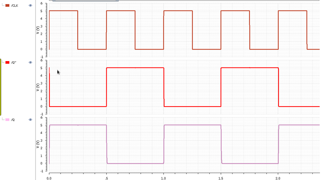
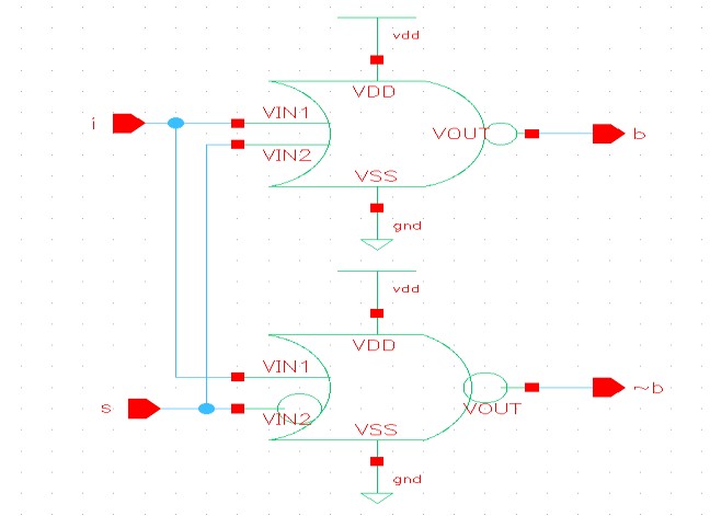
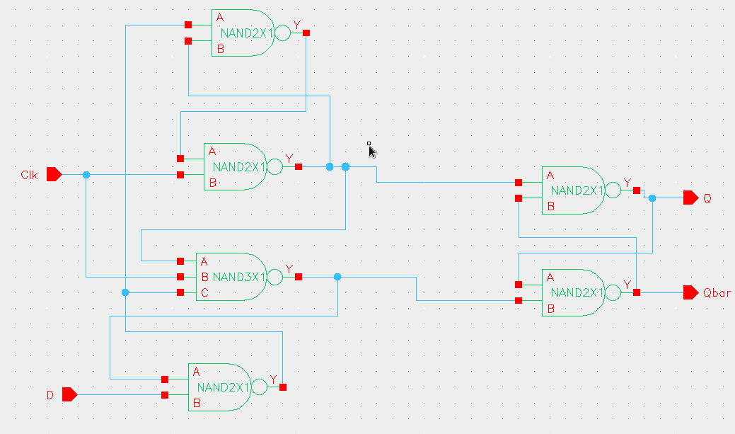
Synchronous Complementary Output D Flip-Flop

|
This is the original design of our transmission gate signal driver. The difference in clock edge from the input versus the inverter may cause the PMOS transistor of the transmission gate to be switched at a later time than the NMOS. To prevent this from happening, we decided to try and use a synchronous D flip-flop. The DFF in the standard libraries don’t provide a true synchronous output that we need. So we had to design a DFF at the gate level.
|
|
In order for the switches to work correctly and synchronously, a synchronous input is required. a synchronous D-Flip flop should be sufficient to provide a synchronous complimentary switch signal.
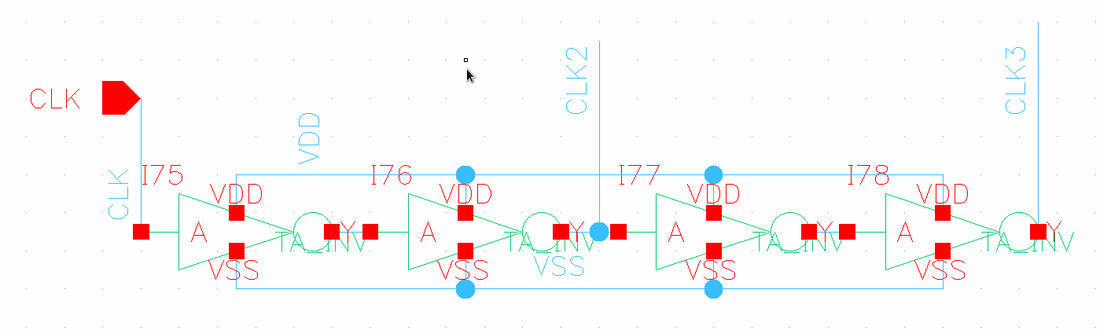
Connected as a clock divider, we used the synchronous DFF to generate our complimentary signals for the switches. 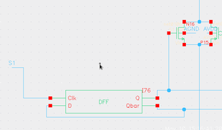
|
|
DAC Performance
DAC Testbench
|
DAC Testbench Input
Voltage Output vs. Digital Input.
|

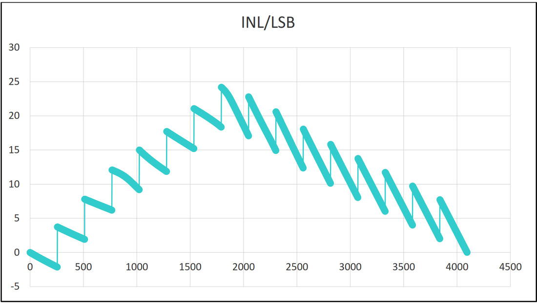
Integral Non-linearity
|

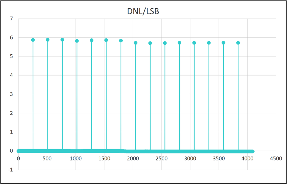
Differential Non-linearity
|
Comparator
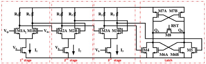
The comparator design consisted of four different stages. The first three are pre-amplifiers to amplify the difference in the two input signals. The last stage is a latch with a hysteresis loop to prevent switching from noise and to only change on a clock edge.

Comparator Stages Illustration
To create a comparator that will compare two voltages, we needed to amplify the input differential voltage to make it a binary signal. The quality of the signal does not matter as much as an operational amplifier because the signal is meant to clip to the positive and negative rails.

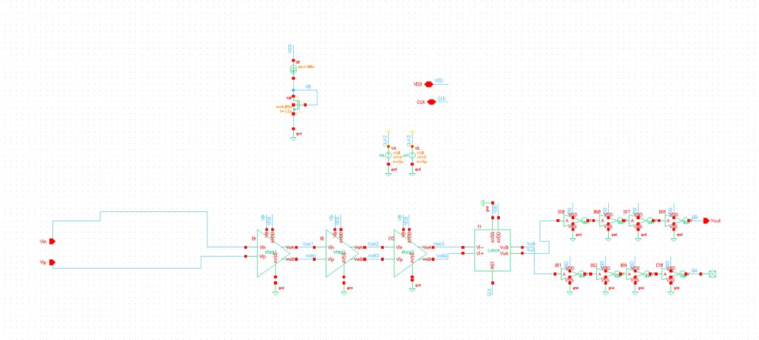
Comparator Module
Pre-Amp(s)
|
Here is the schematic of the test-bench for my pre-amp.
The Preamp stages has the following configuration with different sizing. The first stage having the largest and the last stage having the smallest sizing. 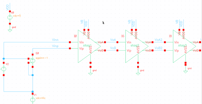
Pre-Amp Testbench
|
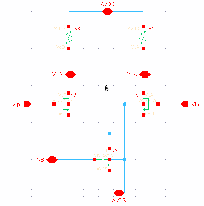
Pre-Amp Module Schematic
|
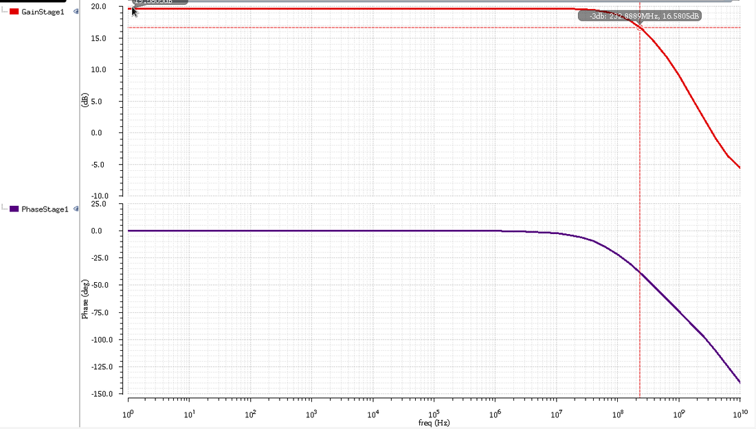
Stage 1 Pre-Amp Bode Plot
|
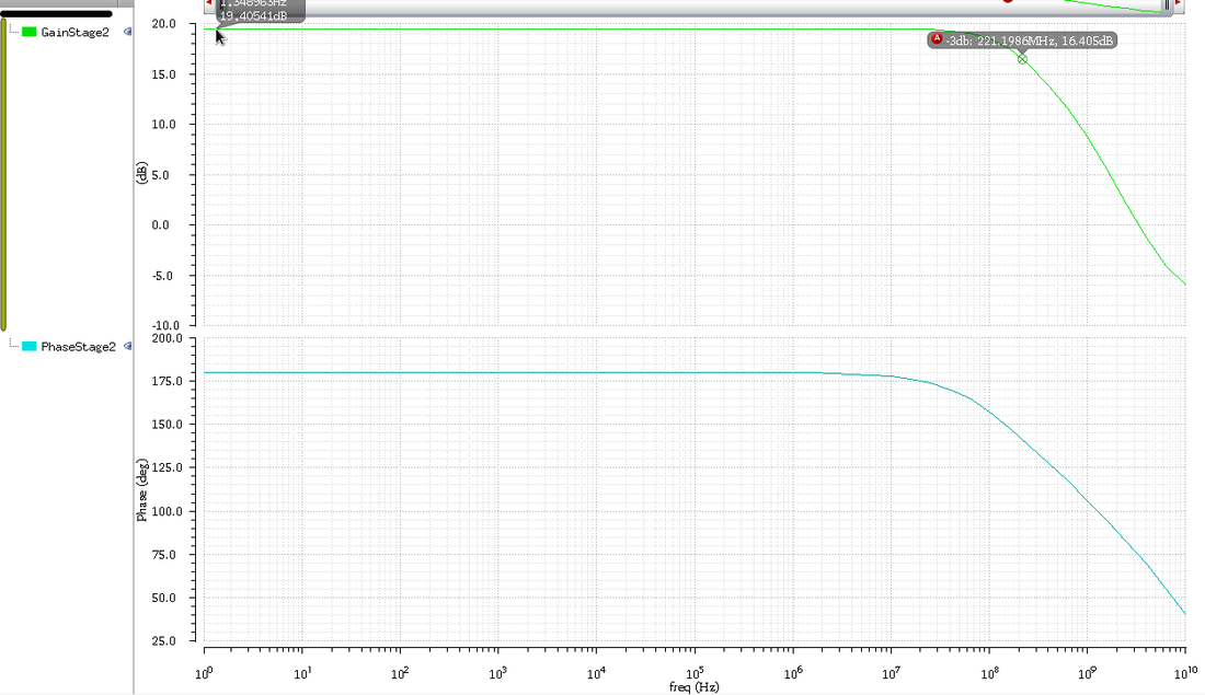
Stage 2 Pre-Amp Bode Plot
|
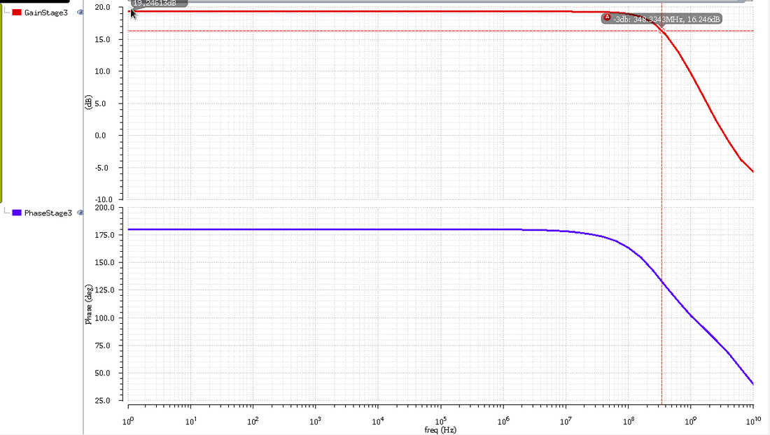
Stage 3 Pre-Amp Bode Plot
|
Latch
The latch with a hysteresis loop is a sub-component of the comparator. In order to switch the comparator only on a positive clock edge, we use a latch.
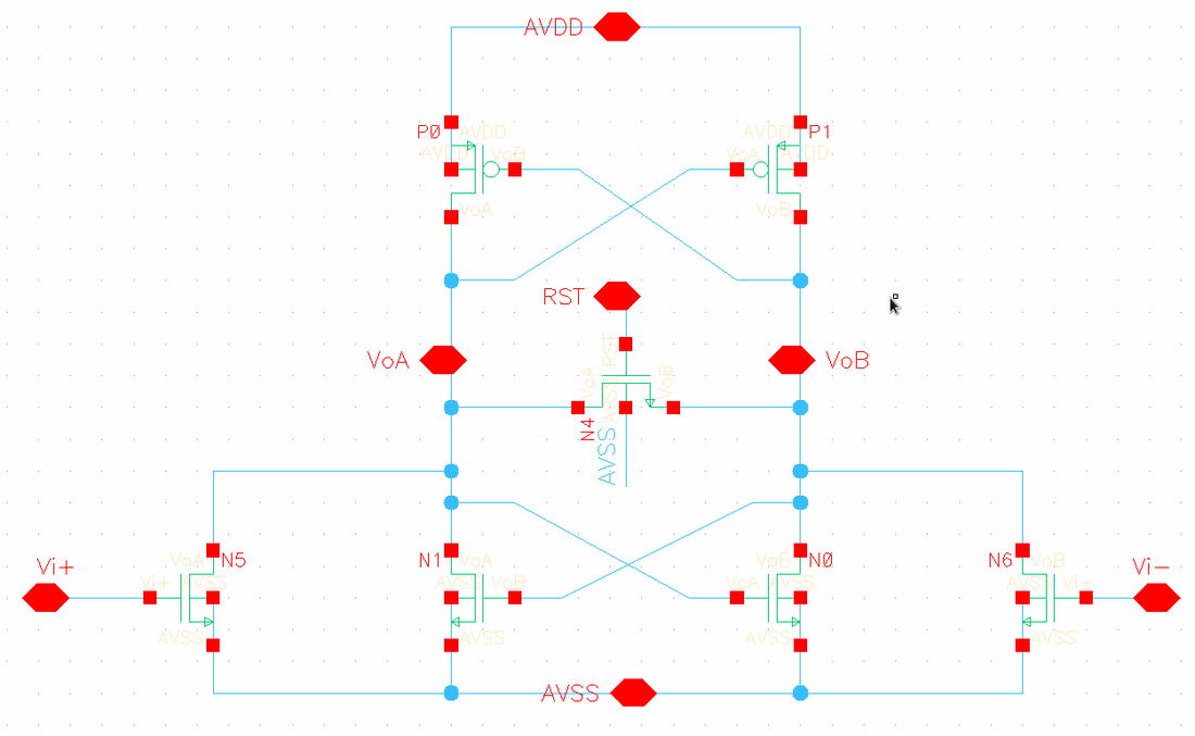
Latch Schematic
|
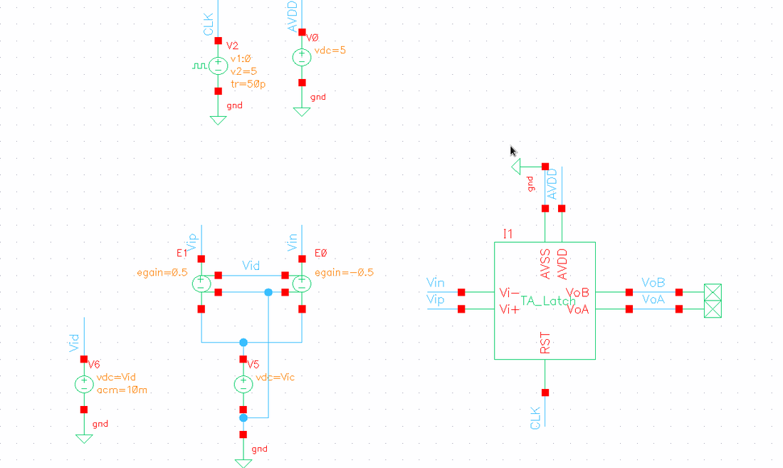
Latch Testbench
|
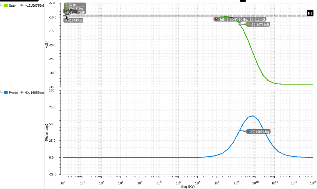
Latch Bode Plot
Latch Propogation Delay
Overall Comparator Test
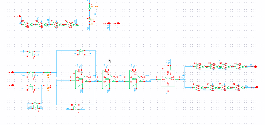
Entire Comparator Testbench
|
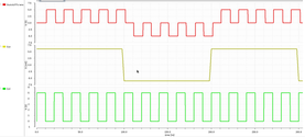
To simplify the inputs of the comparator, I added a delay circuit with four inverters as shown below:
With this circuit, we only needed one clock input.
|
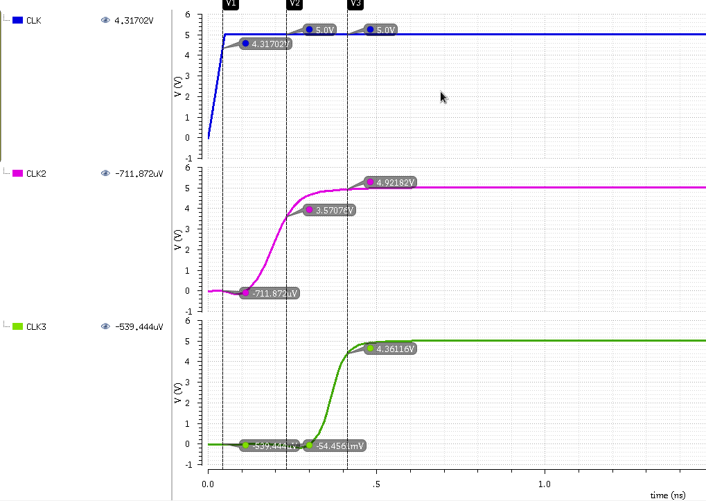
Clock delay from inverters.
|
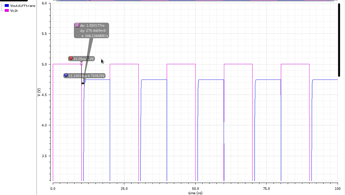
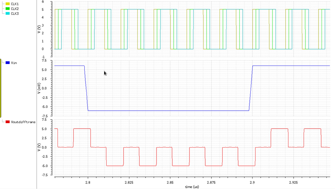
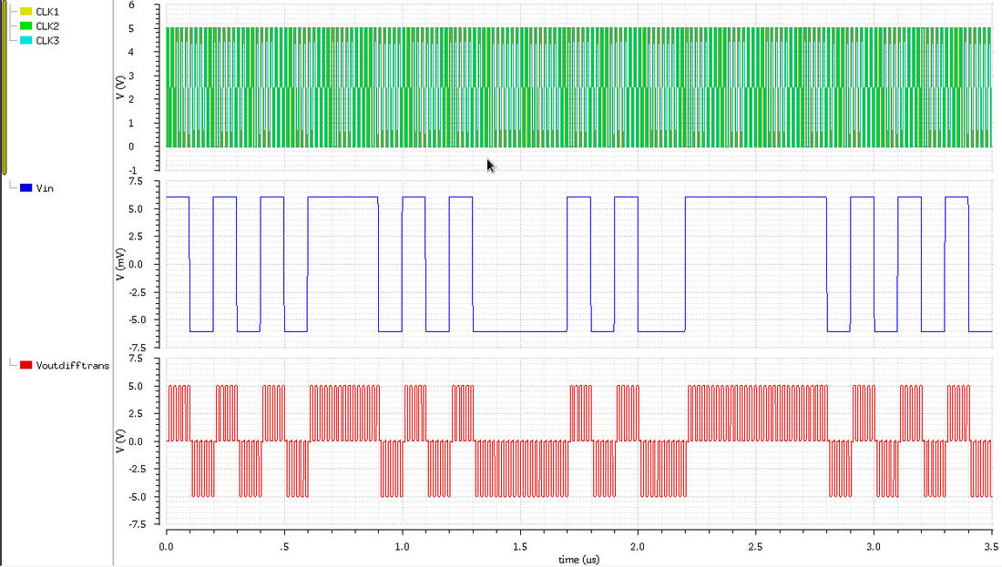
Below are the tests for the overall comparator. As we can see, the comparator operates as desired.
|
|
|
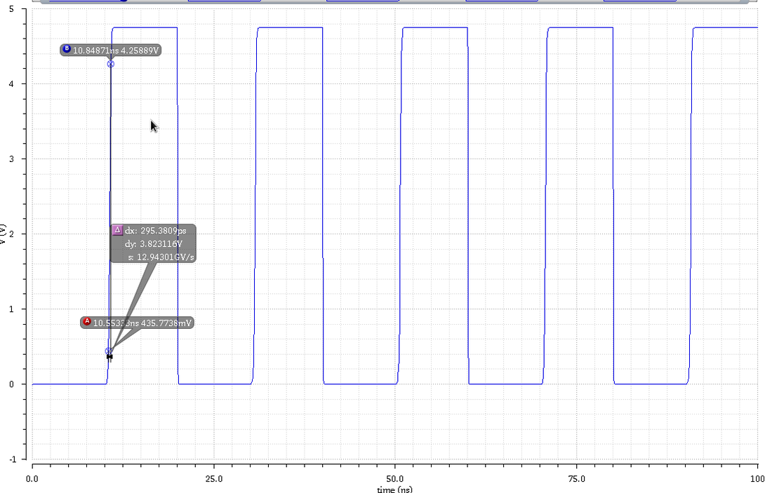
Comparator Slew Rate
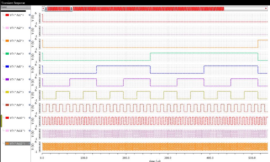
Successive Approximation Register Logic
|
In the SAR digital controller, there is four states:
1.wait [0,0] 2.sample [0,1] 3.convert [1,0] 4.done [1,1] The next state is determined by the previous state and the 'go' signal which is input by the user to indicate that a conversion is desired. |
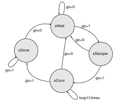
SAR logic state diagram
|
State 1: wait
|
During this state, the last valid result is output. This may not be the valid output because the last valid output may have been from long ago or the ADC may have recently started. from an off-state.
|
State 2: sample
|
In this state, an input is sampled. The sample-and-hold circuit is used to preserve the voltage sampled while the voltage is being converted.
|
State 3: convert
|
The controller repeats the process of changing the switch value starting with the most significant bit and going to the least significant bit to find the digital value to make the DAC output closest to Vin. This is the critical point where the efficiency and speed of the ADC is defined and where the DAC and comparator are put to use.
|
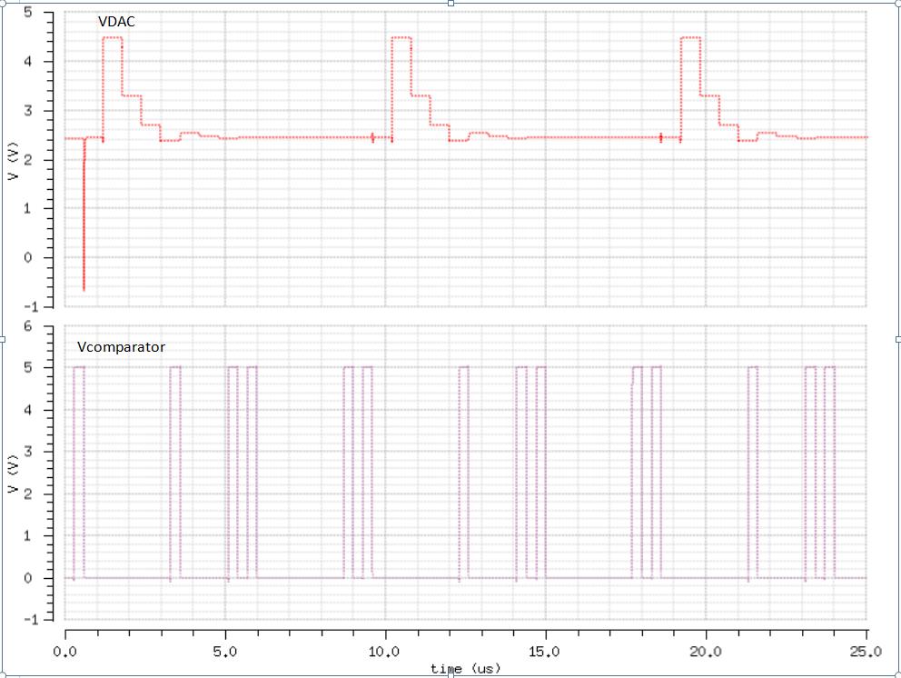
Controller Simulation 2.44V
|
DAC Input Changing as the Control Logic is Looping.
|
State 4: done
|
Once the controller has gone through all bits of the value signal to determine the digital value which causes the output of the DAC to be closest to the analog input, the value is stored in a result register and the valid output pin is set high to indicate a valid output is ready.
|
Overall ADC Results
ADC seperate modules testbench

Overall ADC single module Test Bench
|
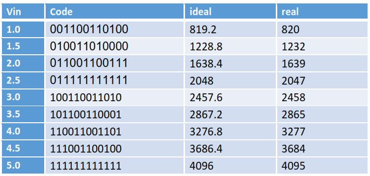
Outputs Vs. Inputs
|
Gallery


Lab Documents
| ee435finalprojectreport.pdf |
