EE 435 Project - Fully Differential Operational Amplifier
Design Goal:
Process: MOSIS ON 0.5 um
Supply: 0V and 5V
Architecture: fully differential two stage, with folded cascade first stage and a single CMFB
1st stage: PMOS input for small noise, gm control by source degeneration
2nd stage: CS amplifier with NMOS input for large gm
CMFB: passive CM detector, diff-pair with NMOS input and PMOS diode load
Bias: PMOS Widlar Iref generator with a single resistor, current mirror bias
Comp: lead compensation
Power budget: <= 2mA * Vdd
Load cap: 2 pF on each output
Specifications:
Large signal: OSR (output swing range): 10% to 90% Vdd for both Vo+ and Vo-
OSR: -85% to +85% for Vod
ICMR (input common mode range): 0% to 70% Vdd
Slew Rate: SR+, SR- >=100 V/uV, at both Vo+ and Vo-
SR+, SR- >=200 V/uV, at both Vod
Small signal: Avd(0) > 90 dB
GBW >= 30 MHz
Small step response percentage overshot: <= 15% for gain=-1
(Phase Margin at unity gain frequency of Ab: >=55o)
0.1% settling time < 200 ns for small step response
Design Overview
The architecture we were assigned to use was a 2-Stage Folded Cascode Op-Amp With a Widlar Iref Generator.
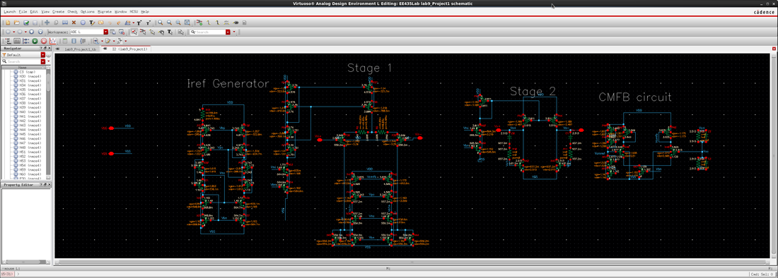
The Op-Amp design can be broken down into four subsections: The current generator, the first amplification stage, the second amplification stage, and the feedback circuit. All of these subsections are shown below:
The Op-Amp design can be broken down into four subsections: The current generator, the first amplification stage, the second amplification stage, and the feedback circuit. All of these subsections are shown below:
Current Generator
|
Stage 1
|

Stage 2
CMFB
|
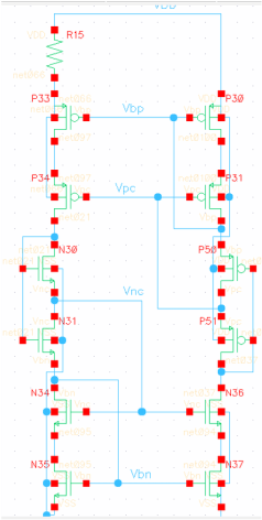
Reference Current Generator (Widlar)The Widlar current generator must have a very reliable current. I decided to use a current of 10 uA(on each side) for the Widlar structure. This would provide me with a good solid base for the op-amp design because it is a nice round number and it is a multiple of 10. Current mirrors will be easy to make because It would just be 10*Multiplier uA for the second side current.
The reference current generator is a very important part of the circuit. In order to design this, I first started with minimum size transistors. Then, I changed the multipliers according to Dr. Chen's suggestion for the structure. After sizing P33 to 4xW of the other PMOS and sizing P50 and N31 to 4xL of all other transistors, the structure worked. And I adjusted the base W for the PMOS transistors until the current was 10uA. I also changed the W of the other NMOS so they had 2xWmin. Later on, I changed the width of some of the NMOS transistors but that didn’t change the current much. This was done to bias other parts of the circuit correctly. |
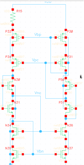
Iref Generator Schematic
|
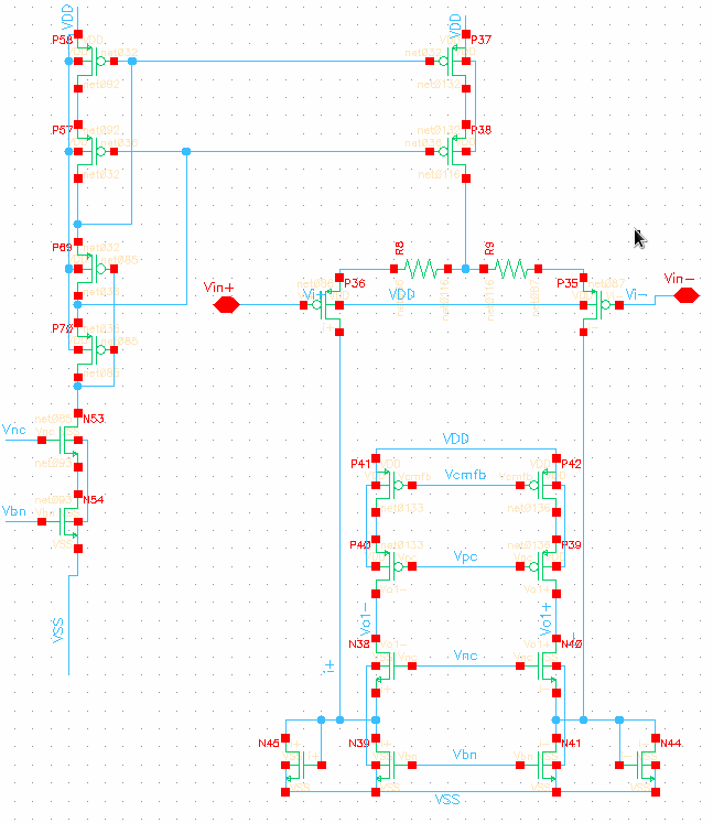
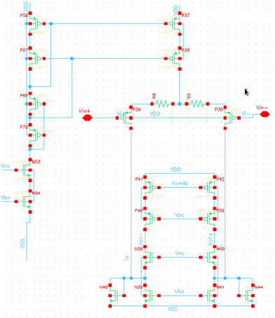
First Stage Schematic
|
First StageTo the left is the schematic of the first stage of my amplifier. In order to design this, I decided on a quiescent current in each branch. For the tail, I decided on 100uA so that each input transistor would have 50uA of current. This makes the current mirror easy because all I would have to do is have a multiplier of 10 on the tail transistors.
For the other stage of the folded cascade, I would need about 10uA of current to keep the gain high. As suggested by Dr. Chen, I inserted a voltage source to isolate this part of the circuit and fixed the Vo1+ and Vo1- at its fixed quiescent voltage of 1V. Then I sized the PMOS transistors and NMOS transistors separately before joining the two and removing the voltage source. This worked pretty well but if I changed something else in the circuit, I would have to isolate them and re-size again. The two bottom NMOS of the folded cascode would then need to have a quiescent current of ~70uAThis was a pretty easy sizing because it is just a multiplier from the widlar structure of 7. |
Second StageThe second stage of my op-amp is shown to the right. This stage is a high gain, high current stage with a simple common source structure. The design of this stage is fairly simple. The desired current was 300uA so the current mirror ratio would be 30.
The sizing of the input transistor is not as important but I kept it proportional to the PMOS. |
Second Stage Schematic
|

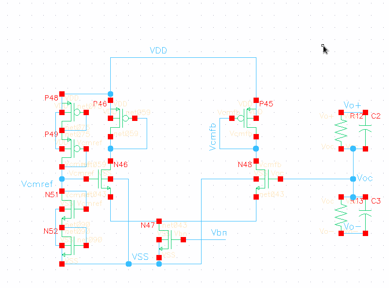
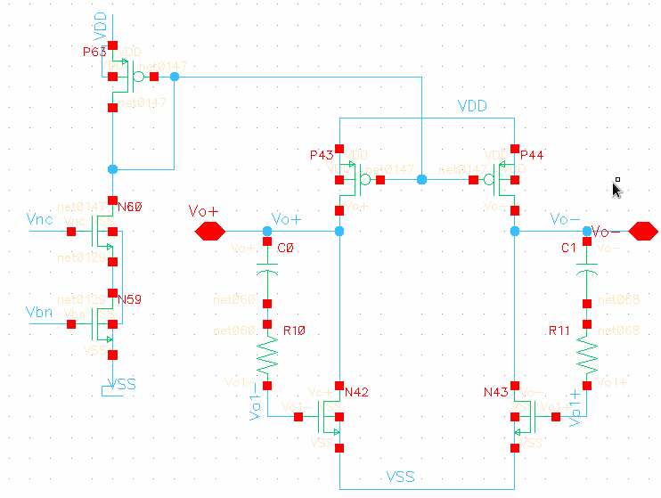
CMFB Circuit
|
Common-Mode FeedbackThis circuit was fairly simple as well. The structure was given and sizing was to be determined by me. The Vcmref circuit to the left is just a Vcmref generator with very small current (about 5nA). The tail transistor was to have 20uA so that each branch could have 10uA so I sized the tail transistor accordingly. Then, the other transistors were fairly simple. Both the PMOS transistors need to be the same size as the PMOS from the first stage in order to bias the circuit correctly.
|
Test Bench Schematic
This is the test bench used. I performed a DC simulation, an AC stability analysis simulation with the differential probe and a transient simulation. The results of these simulations are on the following pages. Vicm was set to 2.5V which is halfway between Vdd and Vss for most simulations.
|
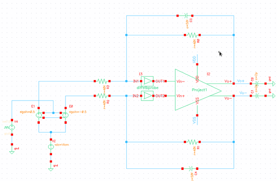
Op-Amp Test-bench
|
Results
|
In the Virtuoso Analog Design Environment, I set the simulator to run a DC, transient and stability simulation as shown in the picture to the right. The plots below are all results of the simulation settings in this image. Each output is computed using the simulation calculator built in to Virtuoso.
|
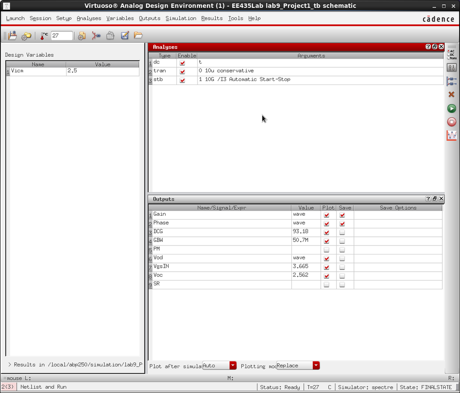
ADE Simulation settings
|
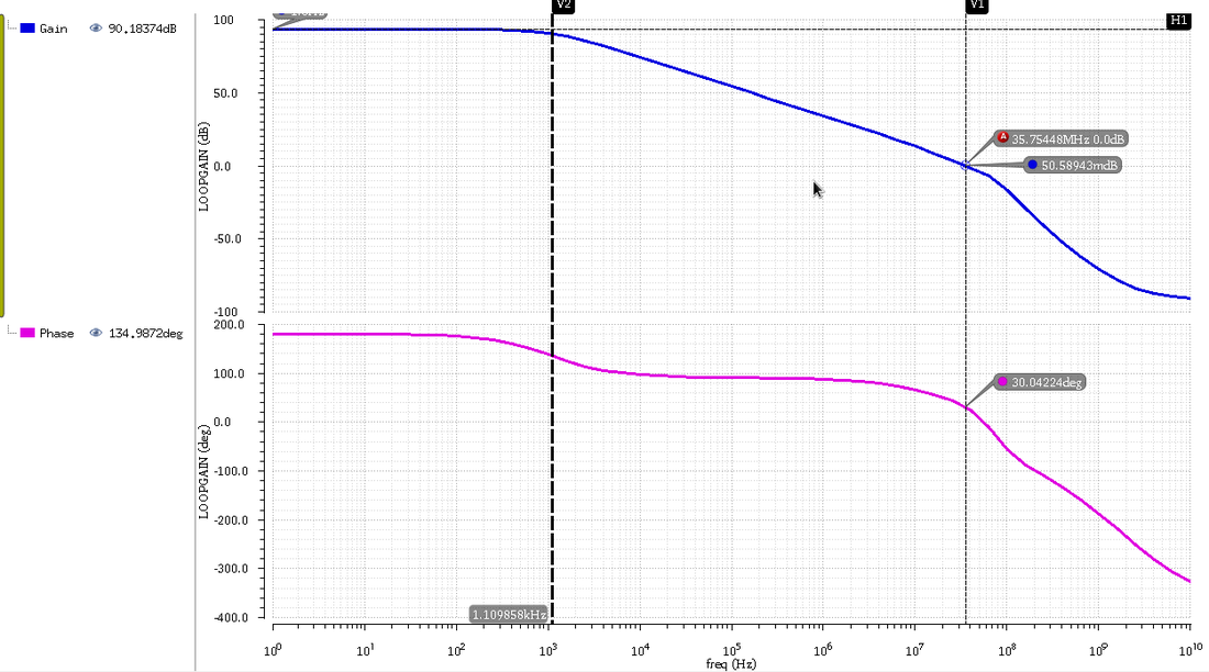
Simulation Bode Plot 1
After I sized everything correctly and I had not yet changed the compensation, I retrieved the above bode plot. This bode plot shows a sufficient DC gain and GBW of 90 and 35MHz respectively. The phase of this circuit is unacceptable and the compensation network must be adjusted.
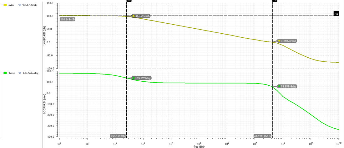
Simulation Bode Plot 2
After adjusting the compensation according to data analysis, I ran the simulation again and obtained the bode plot above.
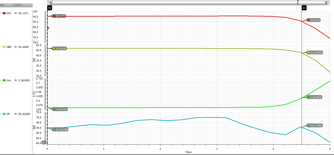
Sweep of Vicm from 0 to 5
This shows that the ICMR is well above the required 4V or 0% to 70%.
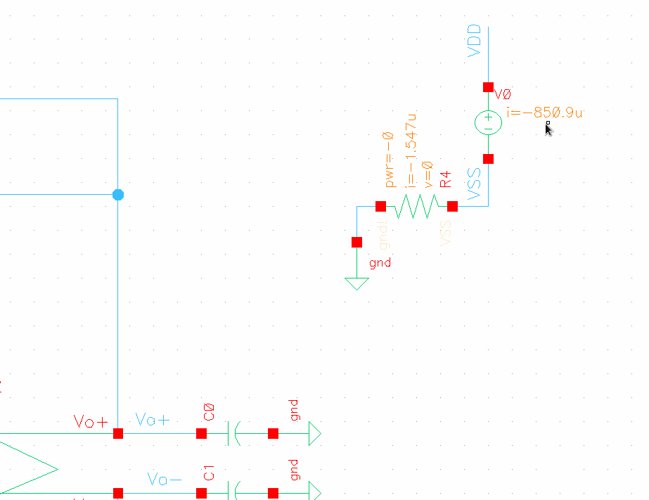
Current Measurement
The total current flowing into the op-amp is .85mA, well below the 2mA requirement.
|
|
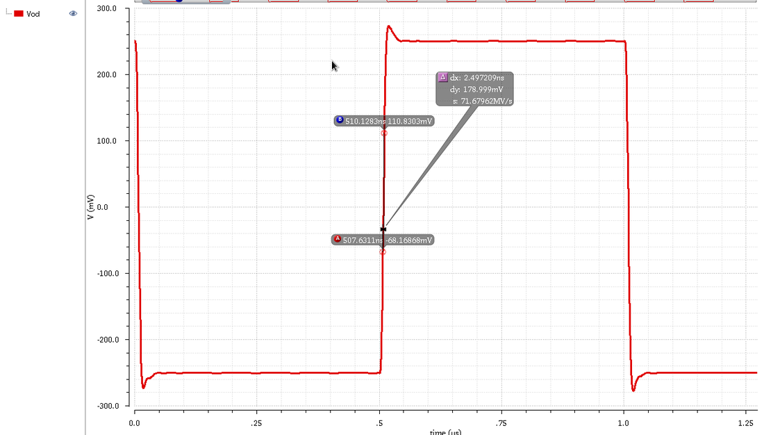
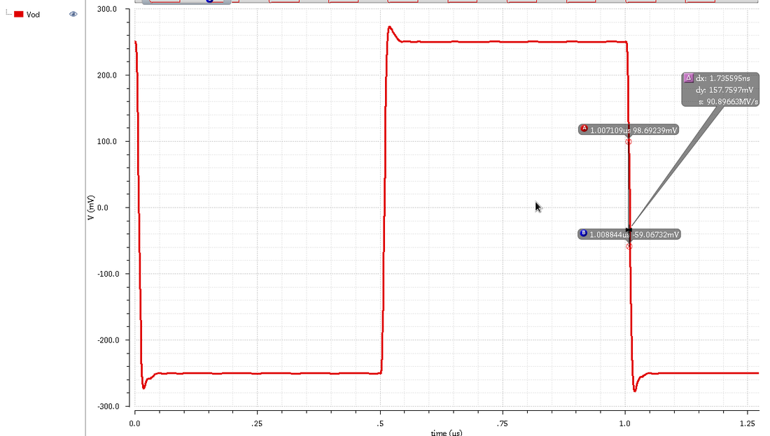
Maximum slew rate was 71MV/S. I was unable to reach the required 100MV/S due to time constraints.
Conclusion
Overall this was a very valuable project and I learned a lot from it. I have always been curious how op-amps work and now I know. It makes me intrigued to learn more about different architectures and configurations.
