Intro
Basic Concept
|
We used the following technology to create the devices:
Thermal wet oxidation Ultraviolet Photo-lithography Wet Etching Diffusion doping with Phosphorous and Boron Physical Vapor Deposition for Metal films (Electron Beam Evaporator) Specifications and DatasheetNumber of blank wafers: 10 Total, 6 Device and 4 Test wafers
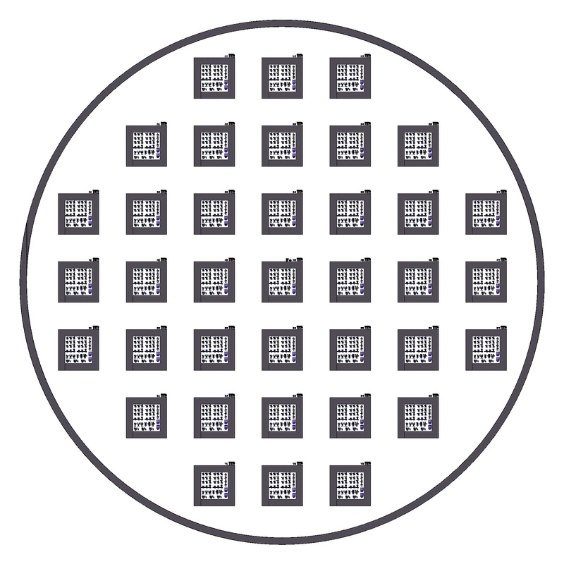
Type: N-type (phosphorous) Resistivity: 1.289Ω*cm Doping Level: 3.63 * 1015 cm-3 Wafer LayoutThere are 37 dies spread out with generous spacing on the wafer as shown in the image to the right. This particular layout has six different masks
|
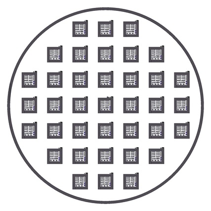
Wafer layout
|

Die layout
|
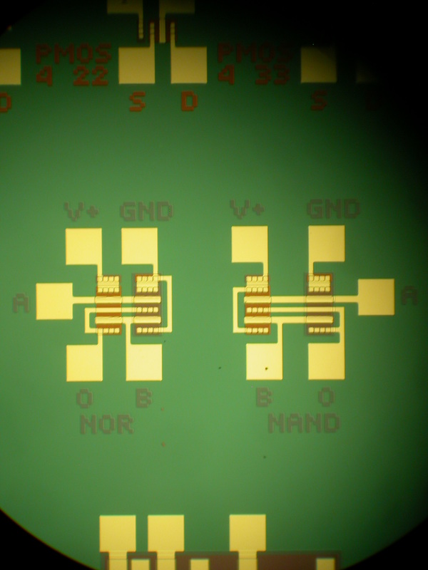
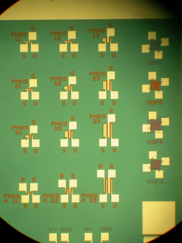
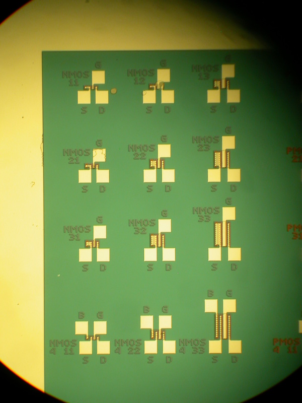
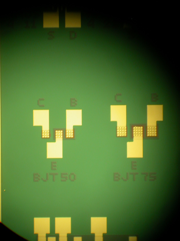
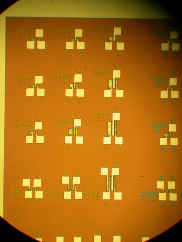
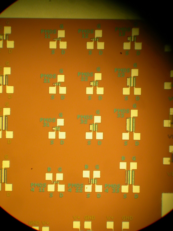
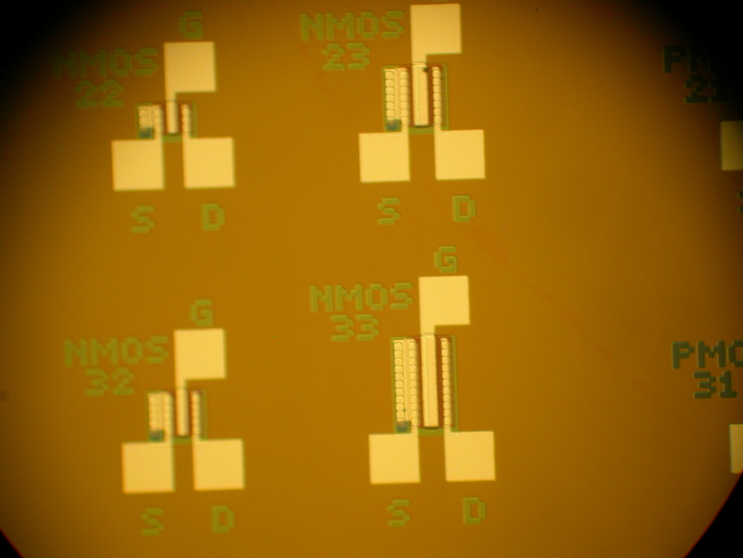
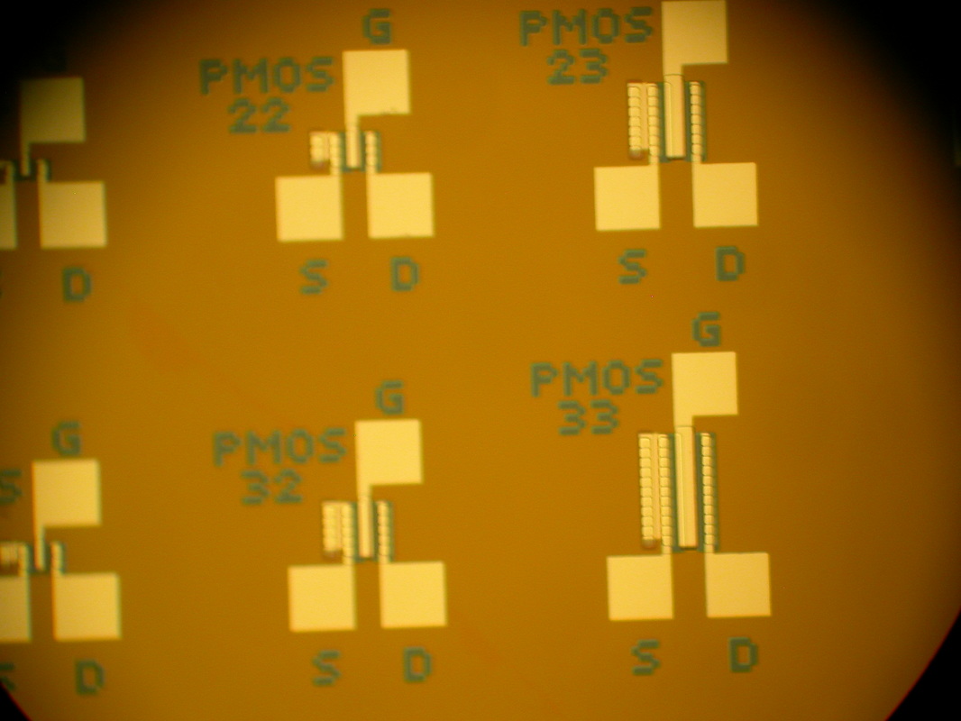
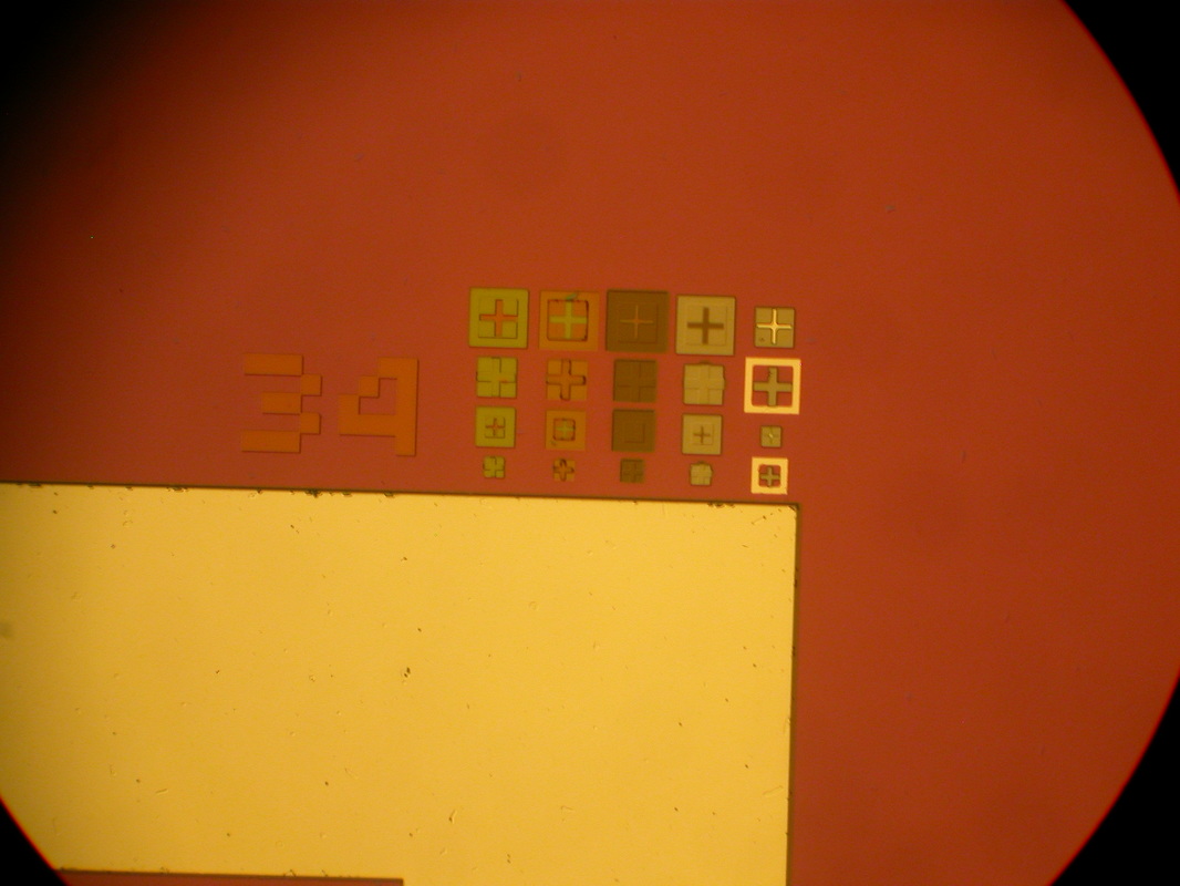
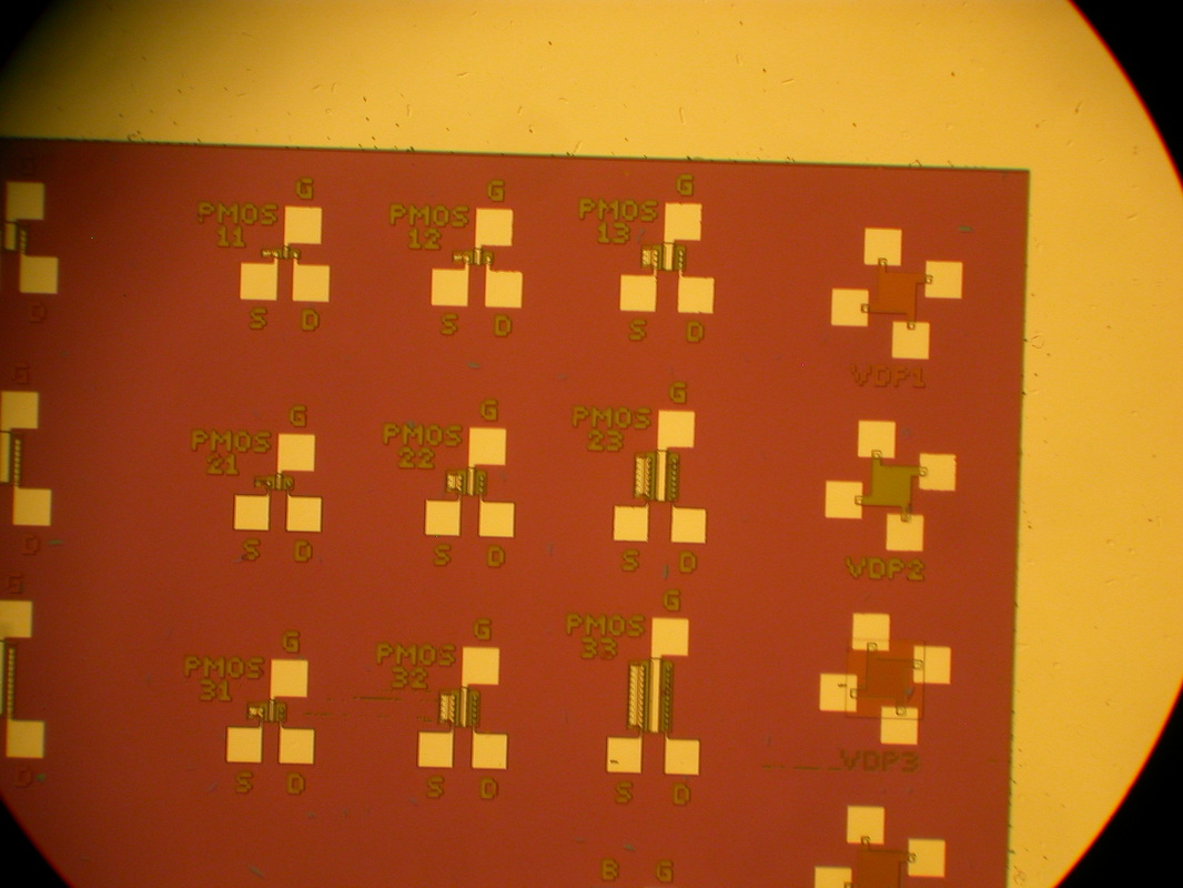
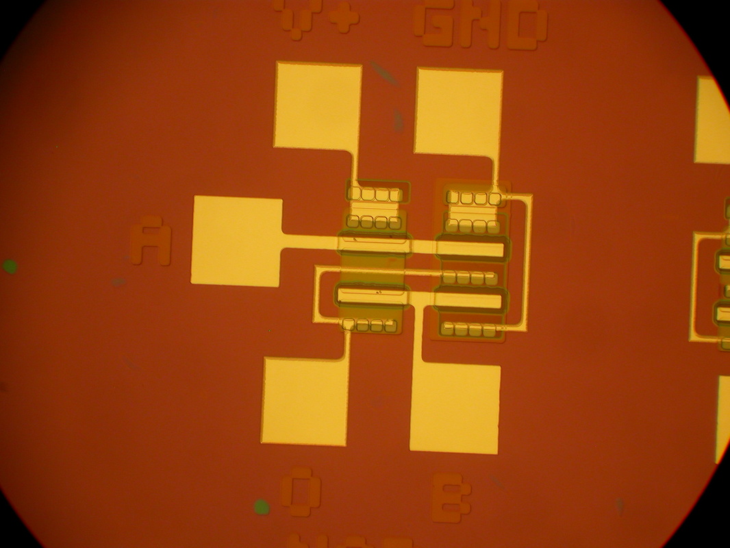
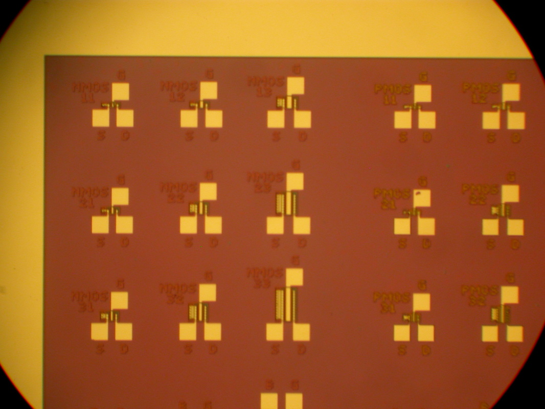
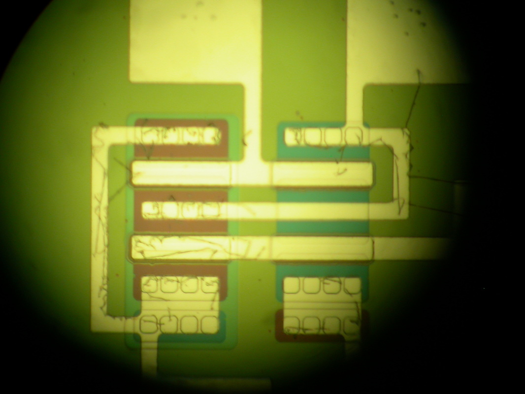
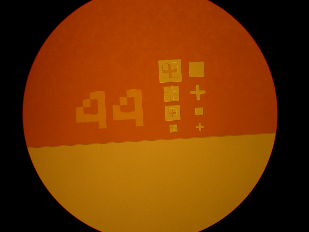
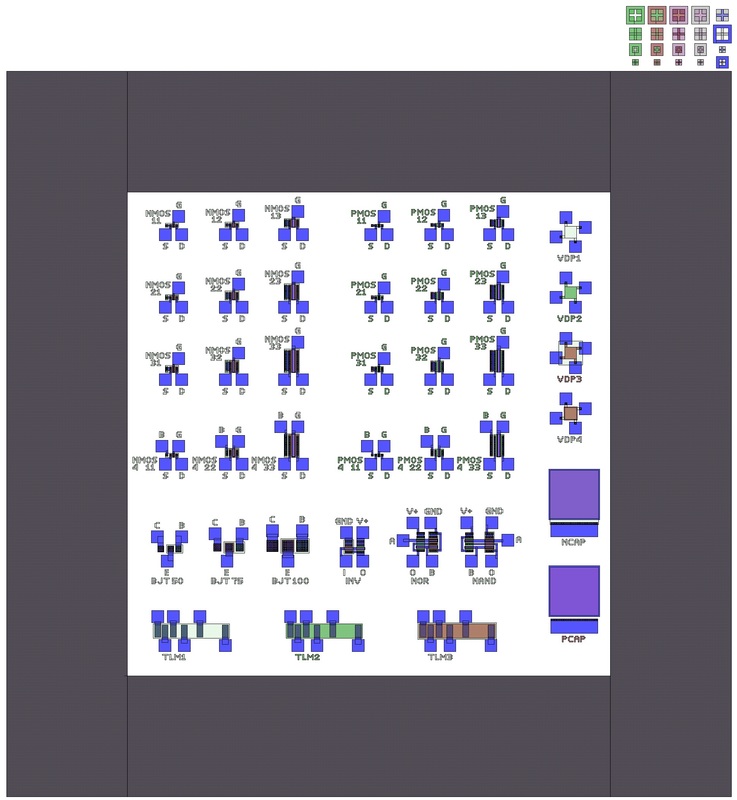
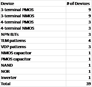
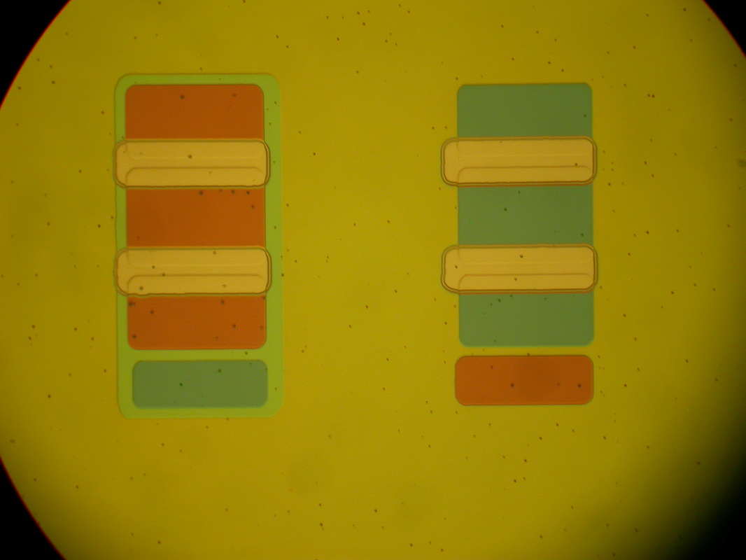
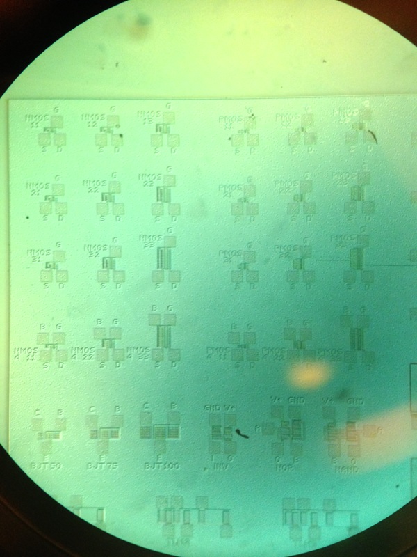
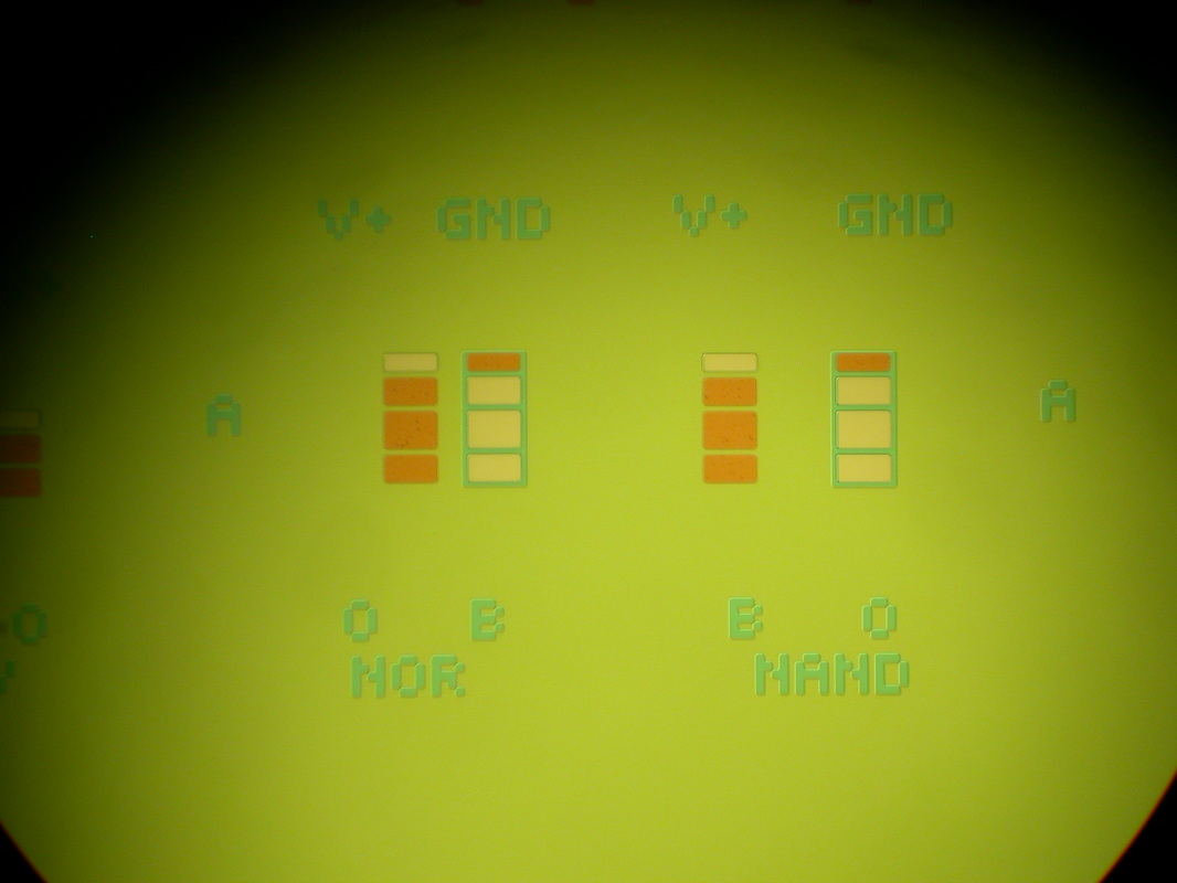
To the left is the layout of each die. Each die contains 39 devices: 12 NMOS transistors and 12 PMOS transistors each of varying sizes along with 3 BJT, an inverter gate, a NOR gate, a NAND gate, three transmission line model structures, four Van-der-Pauw structures, 1 N-capacitor and 1 P-capacitor. These are all meant to test the properties of the material and process. These devices will give us a good idea of the quality of the process we have performed as well as the materials used.

Breakdown of devices on each die
|
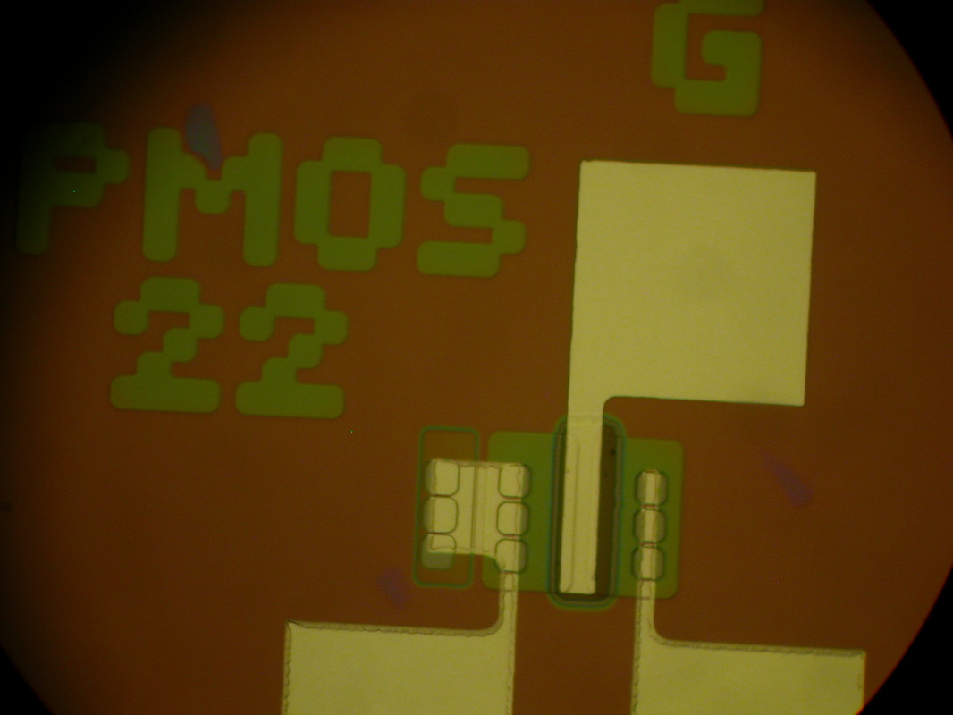
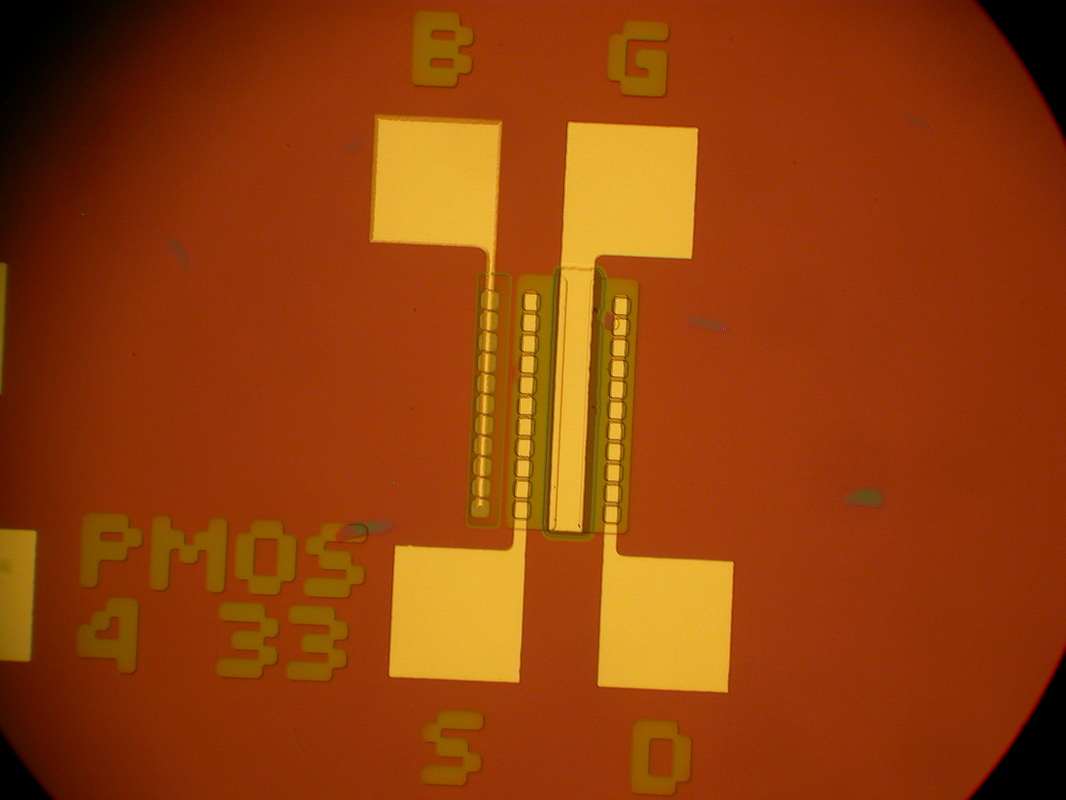
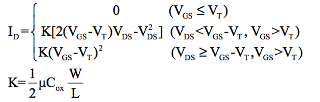
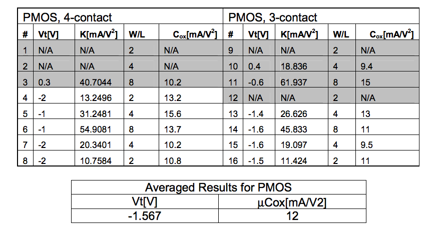
MOSFETs
Channel Widths of MOSFETs
|
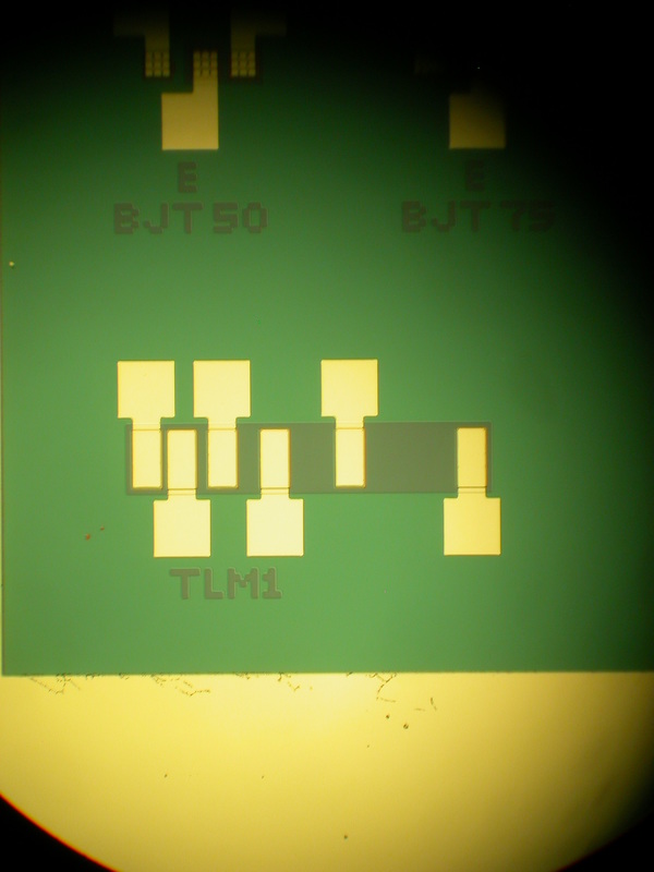
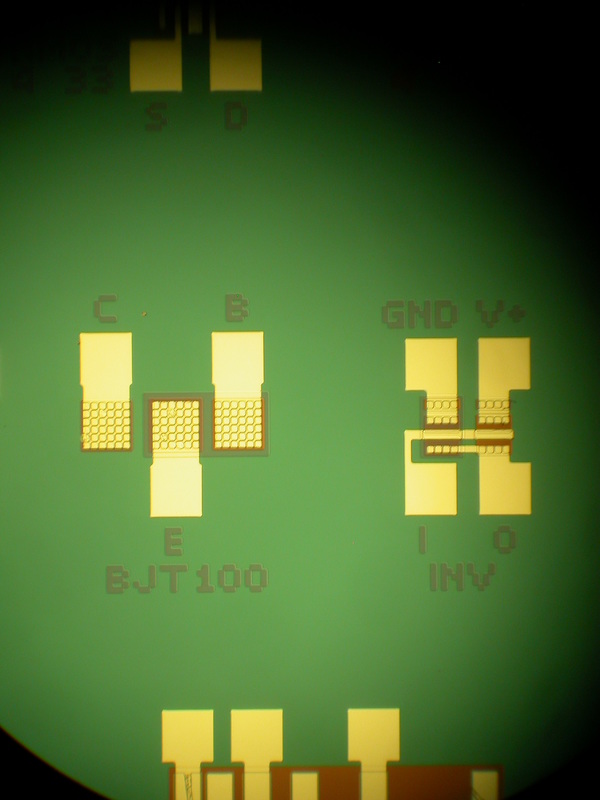
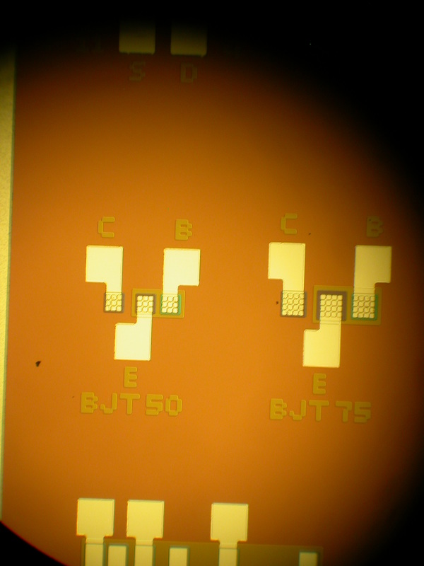
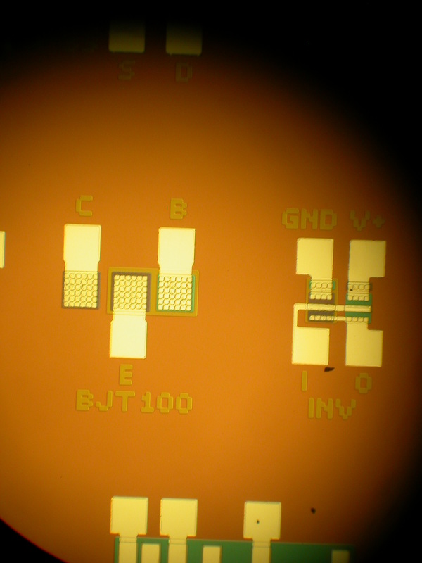
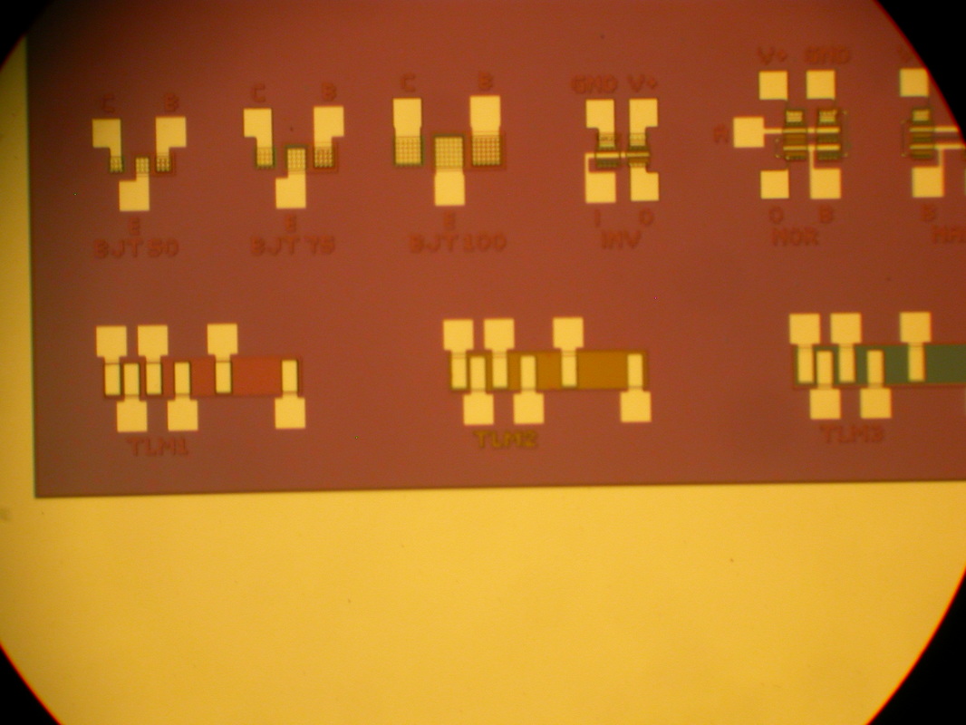
BJTsThere are three sizes of BJTs. They are characterized by their emitter area. The sizes are: 50 𝜇𝑚 by 50 𝜇𝑚, 75 𝜇𝑚 by 75 𝜇𝑚, and 100 𝜇𝑚 by 100 𝜇𝑚.
|
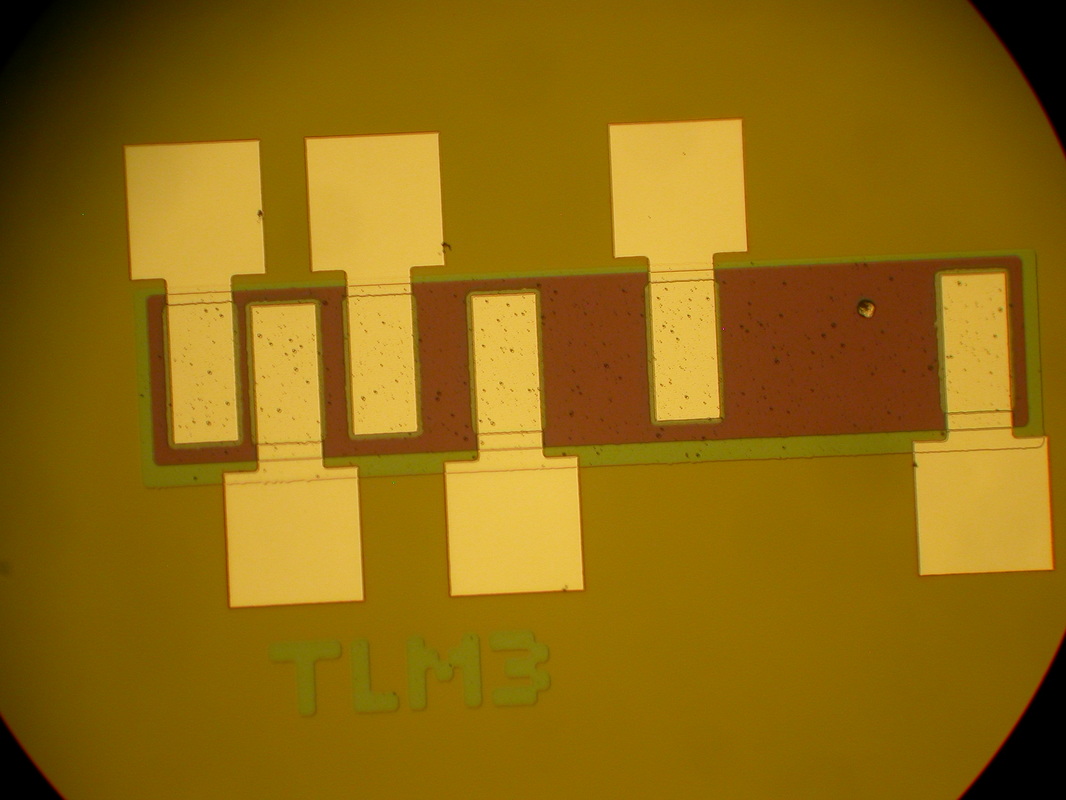
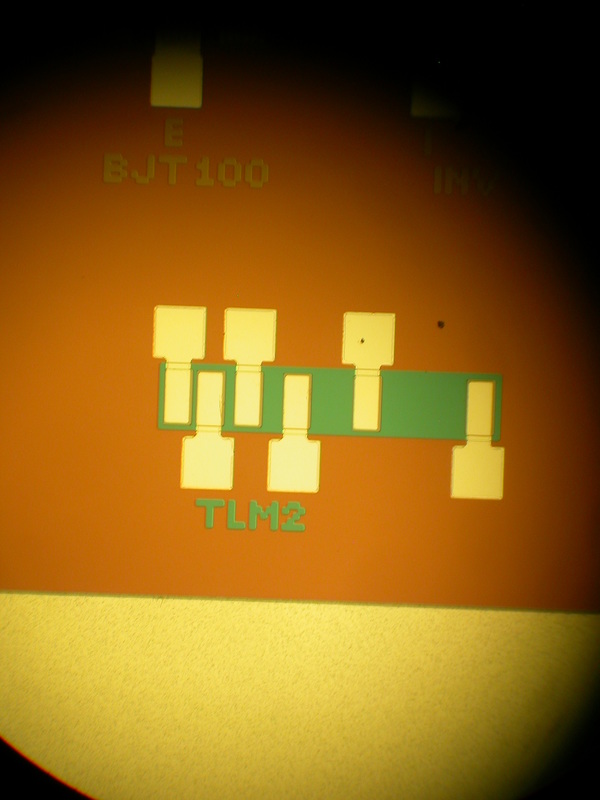
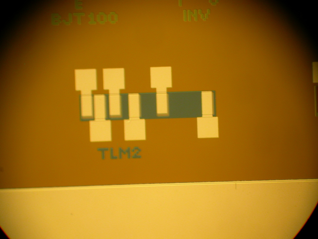
TLM PatternsThe TLM pattern contacts are 50𝜇𝑚 by 100𝜇𝑚. Here are the distances between contacts:
Spacings for TLM
|
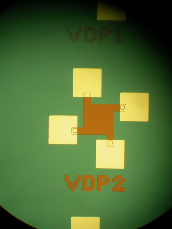
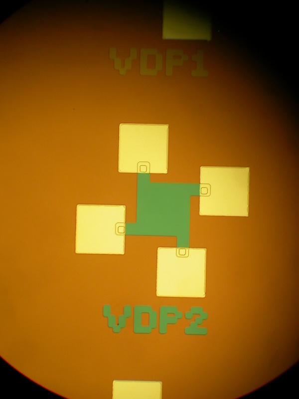
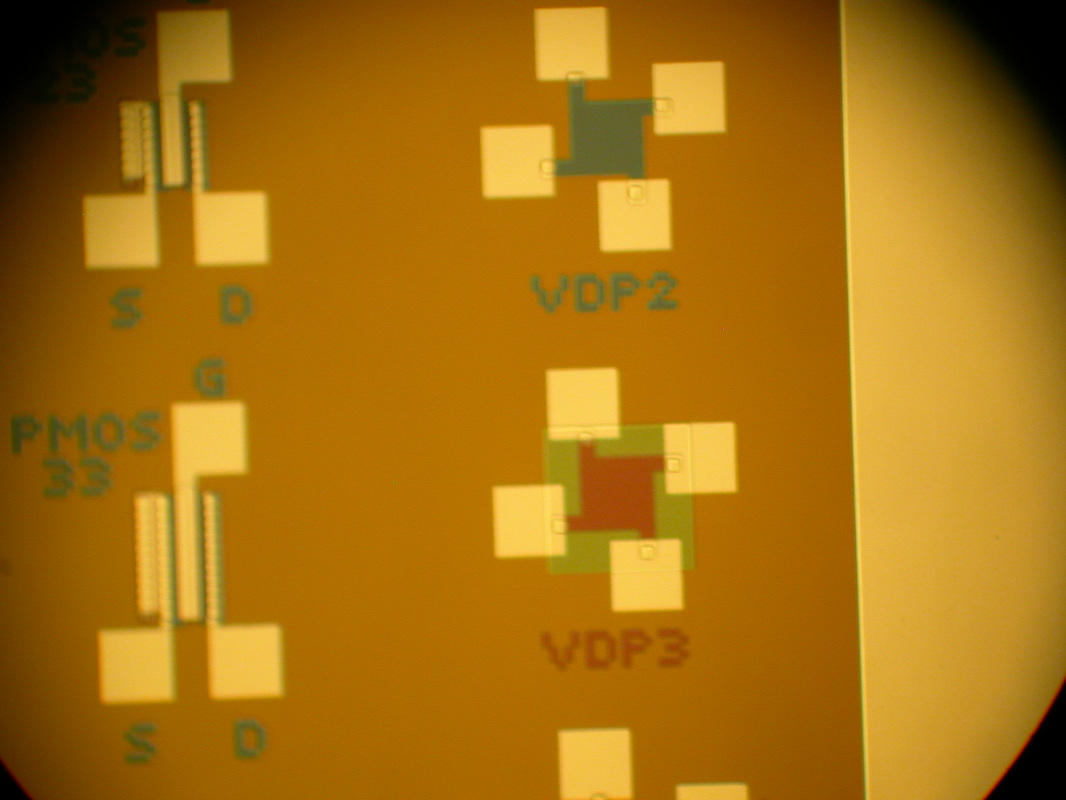
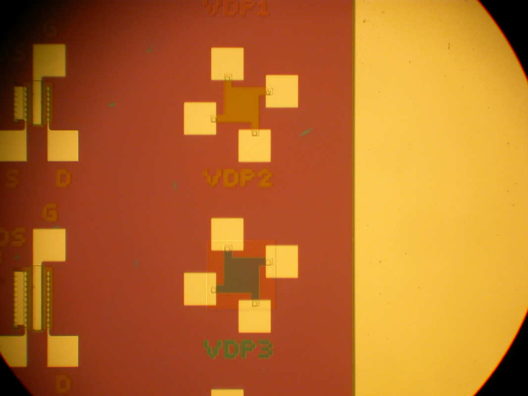
Van der Pauw PatternsThe VDP body is 100𝜇𝑚 by 100𝜇𝑚. Each leg is 20𝜇𝑚 wide with a single contact.
|
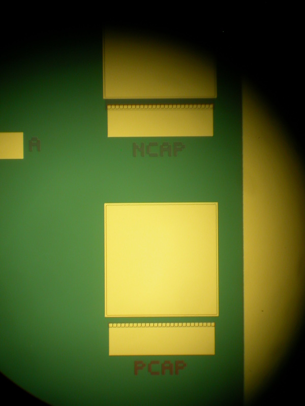
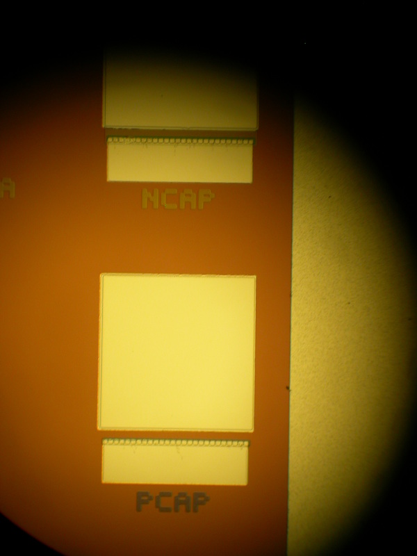
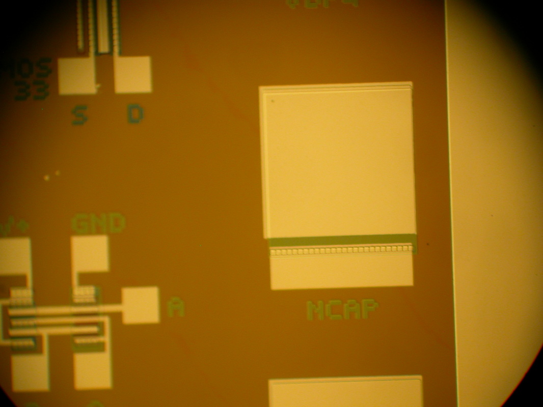
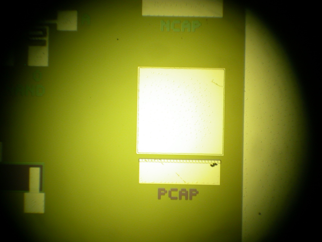
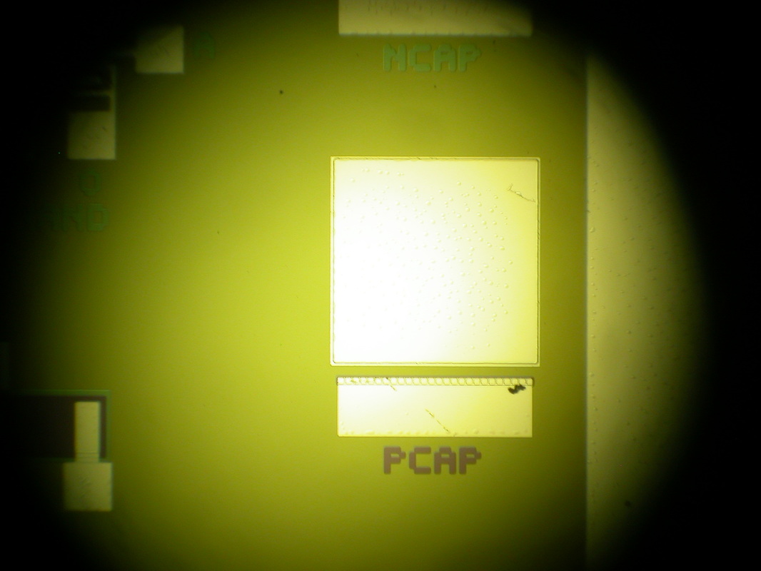
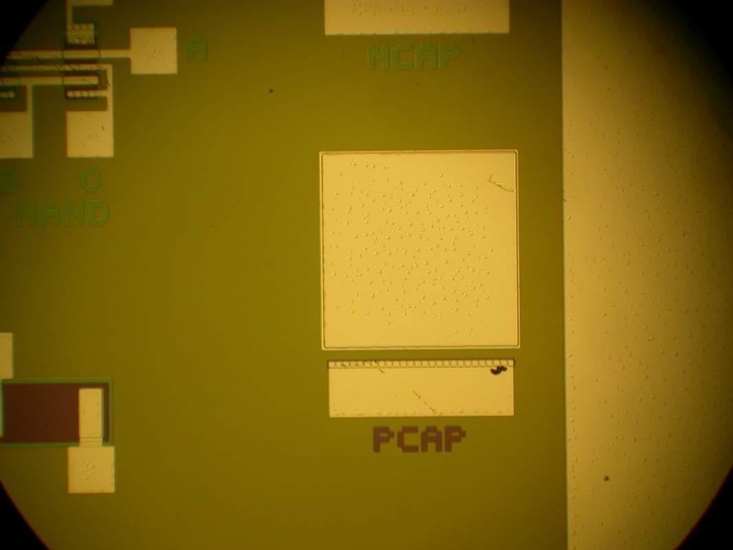
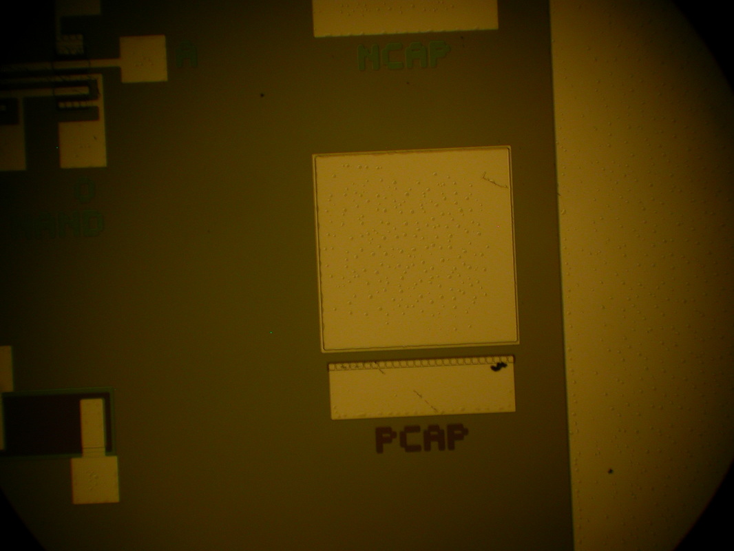
PMOS and NMOS CapacitorThe area for each capacitor is 400𝜇𝑚 by 400𝜇𝑚.
|
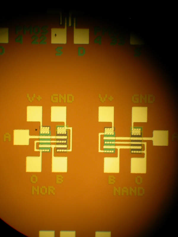
NAND, NOR, and InverterAll the transistors in the NAND, NOR, and Inverter have a channel length of 10 𝜇𝑚 and a channel width of 65 𝜇𝑚.
|
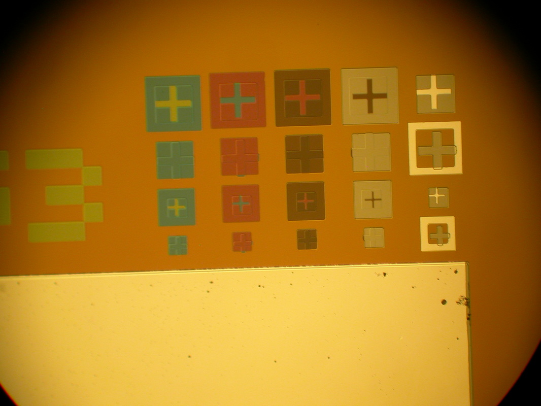
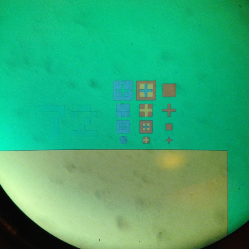
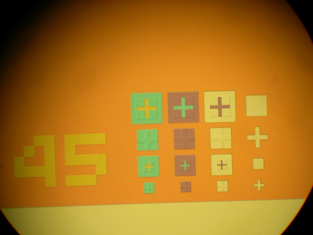
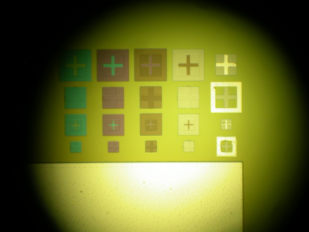
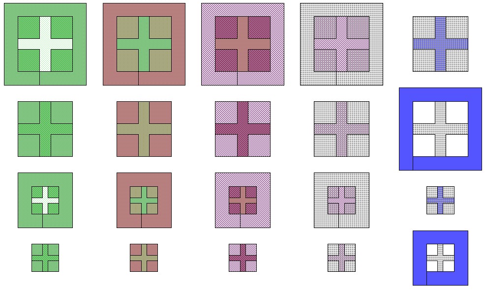
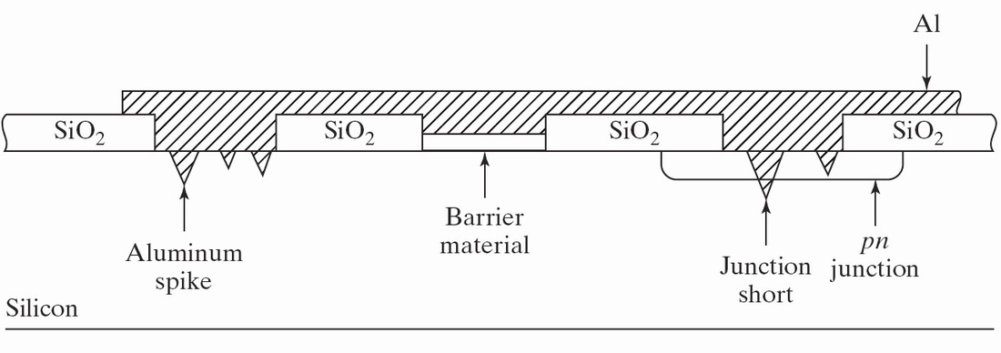
Alignment Marks
|
We have been privileged to experience manually aligning each mask! To do this, there are special alignment marks which are matched with the marks made by the previous layer. These are shown to the right.
Quoted from CyMOS Documentation: There are 4 different sets of alignment marks in the top right corner of each die. Half of these sets use a plus-sign type alignment, while the other half uses a square type alignment. The alignment begins with the p-well layer, either showing up as a plus or a square. This sets the initial alignment that the next mask will line up next to. The PMOS layer will then be lined up to the p-well layer, matching the square to the plus-sign, and the plus-sign to the square. This layer will also add a new plus-sign and square to be used to line up the next mask. This process goes on until the metal layer, where there will not be an extra mark at the end. |

Alignment Features
|
Standard
Clean (RCA clean, Repeated for some other processes)
The purpose of the
standard clean is to eliminate any contaminants before and in-between important
process steps like oxidation and deposition.
Steps:
1.
SC(Solvent Clean)-1 :15 minutes of soaking in 2500ml DI H2O + 500 ml
NH4OH + 500 ml H2O2
a.
Removes
organic residue from the wafers
2.
3
minutes cascade rinse
a.
Removes
leftover SC-1 solution
3.
15
seconds HF dip
a. Hydrofluoric acid removes native silicon dioxide from the wafer.
b. Only needs a short time because it reacts quickly.
c. Removes leftover HF.
4. SC-2: 3000 ml DI H¬¬2O + 500 ml HCl + 500 ml H2O2
a. Removes remaining traces of ionic contaminants.
5. 3 minutes cascade rinse
a. Removes leftover SC-2 solution.
6. Spin rinse and dry
a. Ensures
removal of all solution and dries wafers
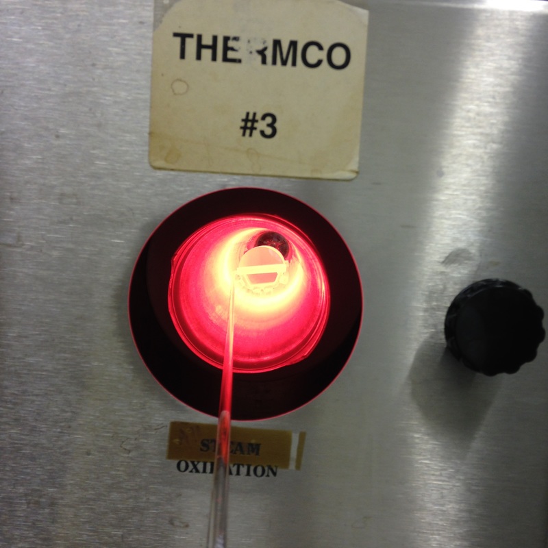
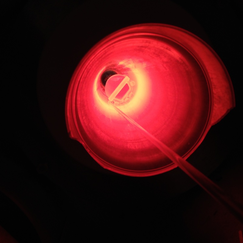
Day 1: Wet Oxidation
The goal of this day is
to create a uniform layer of silicon dioxide on top of the silicon wafer
Steps:
1. Set furnace temperature to 800°C
2. Put wafers in glass boat
3. Push in wafer boat
a. Push at rate of 1 inch every 12 seconds
4. Ramp up temperature
a. Set to 1100°C
b. Waited 22 min to heat up
c. End temp was 1080°C
5. Turn water bubbler on
a. 200 sccm
b. Turn vent on
6. Oxidize
a. Switch N2 to tube
b. Wait 15 minutes
7. Turn water bubbler off
a. Power off bubbler, switch bubbler N2 valve to vent.
8. Ramp down temperature
a. Set N2 flow to 1slpm
b. Turn temperature to 600°C(we are last group of day)
9. Pull out
a. Pull wafer boat at 1 inch per 12 seconds
Oxide thickness
results:
The filmetrics
measurement system measures the film thickness by using an optical spectrometer
to analyze the light reflection off the wafer surface. The film thickness will
determine the reflected light spectrum depending on the material of the film.
The results of the filmetrics system are as follows:
TW1: 285.6nm TW2: 285.5nm TW3: 286.4nm TW4: 284.8nm
Day 2: Photolithography (for p-well)
To create a photoresist
mask pattern on the wafer, we need to coat the wafer with the photoresist and
expose it to UV light.
Steps:
1. Spin HDMS (hexamethyldisilazane) adhesion layer
a. Spins at 4000 rpm for 25 seconds
2. Spin PR
a. A25014E-IR
b. Spins at 4000 rpm for 25 seconds
3. Prebake
a. Cooked on hot plate at 120°C for 1 minute
4. Exposure
a. Exposure machine for 90 seconds
5. Develop PR
a. Soaked In MIF-300 developer for 60-90 seconds
6. Cascade rinse
a. Soaked for 3 minutes to wash off developer
7. Dry
8. Inspect
a. Used microscope to inspect the features on the wafer to make
sure everything went well.
b. They looked good. There were a few contaminations we spotted
but most of the wafers were good.
c. We can also see slight misalignment that may or may not cause
issues.
9. BOE (Buffer Oxide Etch)
a. Submerged the device and test wafer 1 into the BOE solution
until the test wafer 1 was hydrophobic.
b. When the TW1 is hydrophobic, this means it is only silicon on
the surface.
10. Cascade rinse
a. Washes
off excess chemicals
11. Acetone 1
a. Removes photoresist
12. Acetone 2
a. Removes remaining photoresist
13. Methanol
a. Removes acetone and remaining photoresist
14. Cascade rinse
a. Removes remaining chemicals
15. Spin rinse/dry
a. Removes remaining chemicals if any and dries wafers
Day 3: Boron Deposition and Drive
For boron deposition,
we must do a standard clean and perform a deposition step, then a drive step.
Steps:
1.
Standard clean**
a.
All steps from RCA clean.
2.
Place wafers in boat with device side facing boron source
wafers and shield wafers on the other side of device wafers.
3.
Boron Pre-deposition
a.
Push
i.
Temperature at 850°C
ii.
Push at rate of 1 inch / 12 seconds
b.
Recovery
i.
Ambient 1 lpm N2+1 lmp O2
ii.
For 20 minutes
c.
Source
i.
Ambient 1lpm N2 + 1 lpm O2 + 40 sccm H2
ii.
Temperature 850°C
iii.
For 2 minutes
d.
Soak
i.
2 lpm N2 flowing
ii.
850C
iii.
For 50 min
e.
Pull
i.
2lpm N2 850°C
ii.
Pull out at 1 inch / 12sec
4.
Deglaze
a.
BOE
i.
30 seconds
ii.
Takes off oxide layer
b.
Cascade rinse
i.
Takes off chemicals and residue
c.
Spin rinse and dry
i.
Cleans and dries wafers
5.
Standard clean
a.
All steps from part C again
6.
P-well Low -Temp Oxidation and Boron drive
a.
Bubbler on
i.
Temp at 98°C
ii.
200 sccm N2
b.
Push
i.
1 slpm dry N2
ii.
Furnace temp at 800°C
iii.
Rate at 1 inch/12 sec
c.
LTO
i.
200 sccm bubbler N2 vent bubbler to tube
ii.
Temp at 800°C still
iii.
Let sit for 30 mins
d.
Turn bubbler off
e.
Pull
f.
Take wafers out of furnace boat
g.
Deglaze
i.
BOE for 30 seconds
ii.
Cascade rinse
iii.
Spin rinse/dry
h.
Put wavers back in furnace boat
i.
Push
i.
Ramp up
i.
Turn temp to drive temperature
ii.
Turn on bubbler
j.
Wait for furnace to reach drive temp and begin oxidation
i.
Let bubbler vent to furnace
ii.
Wait for desired oxidation time
k.
Bubbler off
l.
Drive
i.
Set nitrogen to 1slpm
ii.
Wait a long time
m.
Ramp down to 800°C or 600°C
n.
Remove wafers
o.
Unload wafers and move to storage bin
Day 4: Photolithography and etching for PMOS
Source and Drain
The photolithography
and etching for the PMOS source and drain was performed by using a mask to
expose a photoresist layer and etching away the oxide underneath.
Steps:
1. Spin HDMS (hexamethyldisilazane) adhesion layer
a. Spins at 4000 rpm for 25 seconds
2. Spin PR
a. A25014E-IR
b. Spins at 4000 rpm for 25 seconds
3. Prebake
a. Cooked on hot plate at 120°C for 1 minute
4. Align and Exposure
a. Align using alignment features with stereoscope.
b. Exposure machine for 90 seconds(Second alignment features)
5. Develop PR
a. Soaked In MIF-300 developer for 60-90 seconds
6. Cascade rinse
a. Soaked for 3 minutes to wash off developer
7. Dry
8. Inspect
a. Used microscope to inspect the features on the wafer to make
sure everything went well.
b. They looked good. There were a few contaminations we spotted
but most of the wafers were good.
c. We can also see slight misalignment that may or may not cause
issues.
9. BOE (Buffer Oxide Etch)
a. Submerged the device and test wafer 1 into the BOE solution
until the test wafer 1 was hydrophobic.
b. When the TW1 is hydrophobic, this means it is only silicon on
the surface.
10. Cascade rinse
a. Washes off excess chemicals
11. Acetone 1
a. Removes photoresist
12. Acetone
2
a. Removes remaining photoresist
13. Methanol
a. Removes acetone and remaining photoresist
14. Cascade rinse
a. Removes remaining chemicals
15. Spin rinse/dry
a. Removes remaining chemicals if any and dries wafers
Day 5: Boron deposition and drive for
PMOS
For boron deposition,
we must do a standard clean and perform a deposition step, then a drive step.
Steps:
1.
Standard clean
a.
All standard clean steps**
2.
Place wafers in boat with device side facing boron source
wafers and shield wafers on the other side of device wafers.
3.
Boron Pre-deposition
a.
Push
i.
Temperature at 850°C
ii.
Push at rate of 1 inch / 12 seconds
b.
Recovery
i.
Ambient 1 lpm N2+1 lmp O2
ii.
For 20 minutes
c.
Source
i.
Ambient 1lpm N2 + 1 lpm O2 + 40 sccm H2
ii.
Temperature 850°C
iii.
For 2 minutes
d.
Soak
i.
2 lpm N2 flowing
ii.
850C
iii.
For 50 min
e.
Pull
i.
2lpm N2
ii.
850°C
iii.
Pull out at 1 inch / 12sec
4.
Deglaze
a.
BOE
i.
30 seconds
ii.
Takes off oxide layer
b.
Cascade rinse
i.
Takes off chemicals and residue
c.
Spin rinse and dry
i.
Cleans and dries wafers
5.
Standard clean
a.
All steps from part C again
6.
P-well Low -Temp Oxidation and Boron drive
a.
Bubbler on
i.
Temp at 98°C
ii.
200 sccm N2
b.
Push
i.
.3 slpm dry N2
ii.
Furnace temp at 800°C
iii.
Rate at 1 inch/12 sec
c.
LTO
i.
200 sccm bubbler N2 vent bubbler to tube
ii.
Temp at 800°C still
iii.
Let sit for 30 mins
d.
Turn bubbler off
e.
Pull
i.
.3 slpm dry N2
ii.
Furnace temp at 800°C
f.
Take wafers out of furnace boat
g.
Deglaze
i.
BOE for 30 seconds
ii.
Cascade rinse
iii.
Spin rinse/dry
h.
Put wavers back in furnace boat
i.
Push
i.
Ramp up
i.
Turn temp to drive temperature
ii.
Turn on bubbler
j.
Wait for furnace to reach drive temp and begin oxidation
i.
Let bubbler vent to furnace
ii.
Wait for desired oxidation time
k.
Bubbler off
l.
Drive
i.
Set nitrogen to 1slpm
ii.
Wait a long time
m.
Ramp down to 800°C or 600°C
n.
Remove wafers
o.
Unload wafers and move to storage bin
Day 6: Photolithography and etching for NMOS
s/d
The photolithography
and etching for the NMOS source and drain was performed by using a mask to
expose a photoresist layer and etching away the oxide underneath. These exposed
regions of silicon will be doped with Phosphorous to create n-type regions.
![]() Steps:
Steps:
1. Spin HDMS (hexamethyldisilazane) adhesion layer
a. Spins at 4000 rpm for 25 seconds
2. Spin PR
a. A25014E-IR
b. Spins at 4000 rpm for 25 seconds
3. Prebake
a. Cooked on hot plate at 120°C for 1 minute
4. Align and Exposure
a. Align using alignment features with stereoscope.
b. Exposure machine for 90 seconds(Second alignment features)
5. Develop PR
a. Soaked In MIF-300 developer for 60-90 seconds
6. Cascade rinse
a. Soaked for 3 minutes to wash off developer
7. Dry
8. Inspect
a. Used microscope to inspect the features on the wafer to make
sure everything went well.
b. They looked good. There were a few contaminations we spotted
but most of the wafers were good.
c. We can also see slight misalignment that may or may not cause
issues.
9. BOE (Buffer Oxide Etch)
a. Submerged the device and test wafer 1 into the BOE solution
until the test wafer 1 was hydrophobic.
b. When the TW1 is hydrophobic, this means it is only silicon on
the surface.
10. Cascade rinse
a. Washes off excess chemicals
11. Acetone 1
a. Removes photoresist
12. Acetone 2
a. Removes remaining photoresist
13. Methanol
a. Removes acetone and remaining photoresist
14. Cascade rinse
a. Removes remaining chemicals
15. Spin rinse/dry
a. Removes remaining chemicals if any and dries wafers
![]() Day 7:
Phosphorus deposition and drive for NMOS
Day 7:
Phosphorus deposition and drive for NMOS
For Phosphorous
deposition, we must do a standard clean and perform a deposition step, then a
drive step.
Steps:
1.
Standard clean**
a.
All standard clean steps
2.
Place wafers in boat with device side facing boron source
wafers and shield wafers on the other side of device wafers.
3.
Boron Pre-deposition
a.
Push
i.
Temperature at 900°C
ii.
Push at rate of 1 inch / 12 seconds
b.
Source
i.
1 lpm N2 flowing
ii.
Temperature 900°C
iii.
For 45 minutes
c.
Pull
i.
2lpm N2
ii.
900°C
iii.
Pull out at 1 inch / 12sec
4.
Deglaze
a.
BOE
i.
30 seconds
ii.
Takes off oxide layer
b.
Cascade rinse
i.
Takes off chemicals and residue
c.
Spin rinse and dry
i.
Cleans and dries wafers
5.
Standard clean
a.
Since we did this in the same day, we did not have to clean
the wafers.
6.
P-well Low -Temp Oxidation and Boron drive
a.
Bubbler on
i.
Temp at 98°C
ii.
200 sccm N2
b.
Push
i.
1 slpm dry N2
ii.
Furnace temp at 800°C
iii.
Rate at 1 inch/12 sec
c.
Ramp up
i.
1 slpm N2
ii.
Temp to 1075°C
iii.
Wait 10 mins
d.
Oxidation
i.
1 slpm H2O
ii.
1075°C
iii.
10 mins
e.
Drive
i.
1 slpm N2
ii.
1075°C
iii.
20 mins
f.
Ramp Down
i.
1 slpm N2
ii.
Set to 800°C
iii.
Wait 8 min
g.
Pull
h.
1 slpm N2
i.
800°C
ii.
1 inch every 12 seconds
i.
Unload wafers and move to storage bin after letting cool
Day 8: Photolithography and etching for gate
oxide
The photolithography
and etching for the PMOS source and drain was performed by using a mask to expose
a photoresist layer and etching away the oxide underneath.
Steps:
1. Spin HDMS (hexamethyldisilazane) adhesion layer
a. Spins at 4000 rpm for 25 seconds
2. Spin PR
a. A25014E-IR
b. Spins at 4000 rpm for 25 seconds
3. Prebake
a. Cooked on hot plate at 120°C for 1 minute
4. Align and Exposure
a. Align using alignment features with stereoscope.
b. Exposure machine for 90 seconds(Second alignment features)
5. Develop PR
a. Soaked In MIF-300 developer for 60-90 seconds
6. Cascade rinse
a. Soaked for 3 minutes to wash off developer
7. Dry
8. Inspect
a. Used
microscope to inspect the features on the wafer to make sure everything went
well.
b. They looked good. There were a few contaminations we spotted
but most of the wafers were good.
c. We can also see slight misalignment that may or may not cause
issues.
9. BOE (Buffer Oxide Etch)
a. Submerged the device and test wafer 1 into the BOE solution
until the test wafer 1 was hydrophobic.
b. When the TW1 is hydrophobic, this means it is only silicon on
the surface.
10. Cascade rinse
a. Washes off excess chemicals
11. Acetone 1
a. Removes photoresist
12. Acetone 2
a. Removes remaining photoresist
13. Methanol
a. Removes acetone and remaining photoresist
14. Cascade rinse
a. Removes remaining chemicals
15. Spin rinse/dry
a. Removes remaining chemicals if any and dries wafers
Day 9: Dry Oxidation for gate oxide
The goal of this Days
to create a uniform layer of silicon dioxide on top of the silicon wafer
Steps:
1. Standard clean**
2. Set furnace temperature to 800°C
3. Put wafers in glass boat
4. Push in wafer boat
a. Push at rate of 1 inch every 12 seconds
5. Ramp up temperature
a. Set to
1100°C
b. Waited 10 min to heat up
c. End temp was 1080°C
6. Turn Oxygen on
a. 1 slpm O2
b. Turn vent on
7. Oxidize
a. Switch N2 to tube
b. Wait 19 minutes
8. Turn O2 off
a. Power off bubbler, switch N2 valve to vent.
9. Ramp down temperature
a. Set N2 flow to 1slpm
b. Turn temperature to 600°C(we are last group of day)
10. Pull out
a. Pull wafer boat at 1 inch per 12 seconds
Day 10: Photolithography and etching for
contact vias
The photolithography
and etching for the PMOS source and drain was performed by using a mask to
expose a photoresist layer and etching away the oxide underneath.
Steps:
1. Spin HDMS (hexamethyldisilazane) adhesion layer
a. Spins at 4000 rpm for 25 seconds
2. Spin PR
a. A25014E-IR
b. Spins
at 4000 rpm for 25 seconds
3. Prebake
a. Cooked on hot plate at 120°C for 1 minute
4. Align and Exposure
a. Align using alignment features with stereoscope.
b. Exposure machine for 90 seconds(Second alignment features)
5. Develop PR
a. Soaked In MIF-300 developer for 60-90 seconds
6. Cascade rinse
a. Soaked for 3 minutes to wash off developer
7. Dry
8. Inspect
a. Used microscope to inspect the features on the wafer to make
sure everything went well.
b. They looked good. There were a few contaminations we spotted
but most of the wafers were good.
c. We can also see slight misalignment that may or may not cause
issues.
9. BOE (Buffer Oxide Etch)
a. Submerged the device and test wafer 1 into the BOE solution
until the test wafer 1 was hydrophobic.
b. When the TW1 is hydrophobic, this means it is only silicon on
the surface.
10. Cascade rinse
a. Washes off excess chemicals
11. Acetone 1
a. Removes photoresist
12. Acetone 2
a. Removes remaining photoresist
13. Methanol
a. Removes acetone and remaining photoresist
14. Cascade rinse
a. Removes remaining chemicals
15. Spin rinse/dry
a. Removes remaining chemicals if any and dries wafers
Day 11: Metallization and annealing
We did not do these
steps because we are not qualified to operate the machine. Our TA did them for
us.
1. Load Samples
2. Power
Up
3. Manual Deposition
4. Power Down and Unload
5. Load wafers into furnace to anneal
6. Ramp up temperature
7. Ramp down temperature
8. Remove Wafers
Day 12: Photolithography and etching for
aluminum contacts/gates
The photolithography
and etching for the aluminum layer which makes the contacts and gate layers. An
aluminum layer has been deposited over the entire wafer and now needs to be
etched away in unwanted areas.
Steps:
1. Spin HDMS (hexamethyldisilazane) adhesion layer
a. Spins
at 4000 rpm for 25 seconds
2. Spin PR
a. A25014E-IR
b. Spins at 4000 rpm for 25 seconds
3. Prebake
a. Cooked on hot plate at 120°C for 1 minute
4. Align and Exposure
a. Align using alignment features with stereoscope.
b. Exposure machine for 90 seconds(Second alignment features)
5. Develop PR
a. Soaked In MIF-300 developer for 60-90 seconds
6. Cascade rinse
a. Soaked for 3 minutes to wash off developer
7. Dry
8. Inspect
a. Used microscope to inspect the features on the wafer to make
sure everything went well.
b. They looked good. There were a few contaminations we spotted
but most of the wafers were good.
c. We can also see slight misalignment that may or may not cause
issues.
9. BOE (Buffer Oxide Etch)
a. Submerged the device and test wafer 1 into the BOE solution
until the test wafer 1 was hydrophobic.
b. When the TW1 is hydrophobic, this means it is only silicon on
the surface.
10. Cascade rinse
a. Washes off excess chemicals
11. Acetone 1
a. Removes photoresist
12. Acetone 2
a. Removes remaining photoresist
13. Methanol
a. Removes acetone and remaining photoresist
14. Cascade rinse
a. Removes remaining chemicals
15. Spin rinse/dry
a.
Removes
remaining chemicals if any and dries wafers
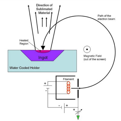
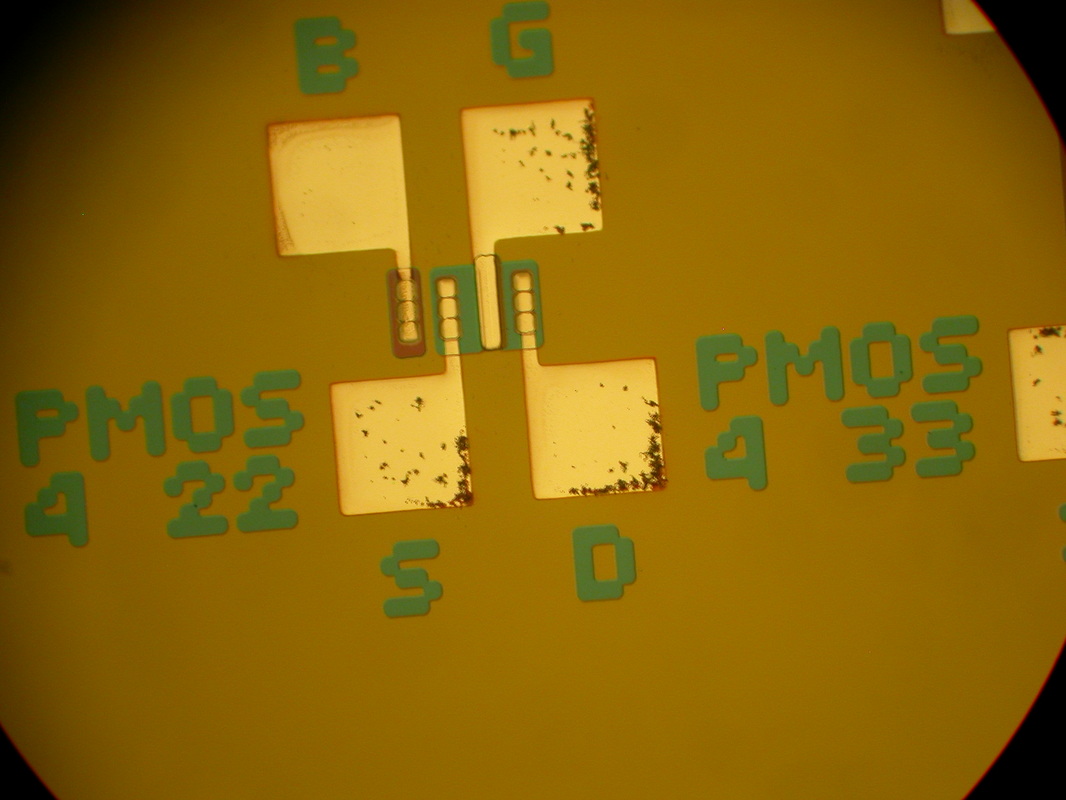
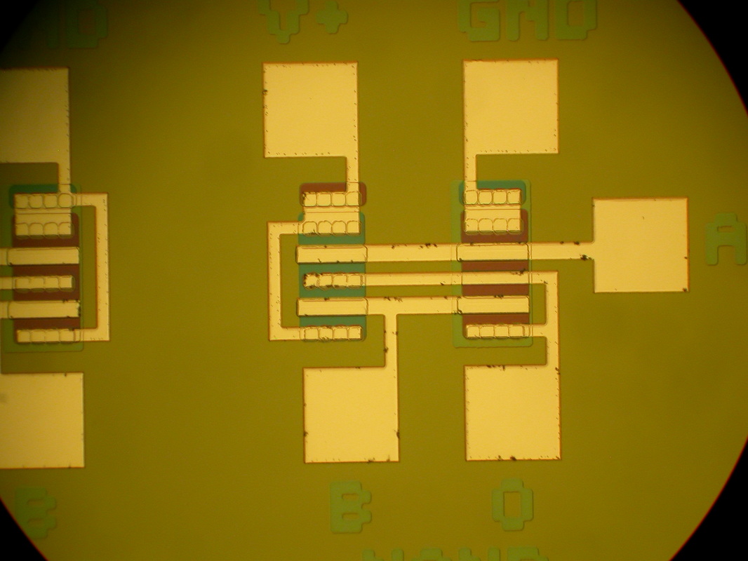
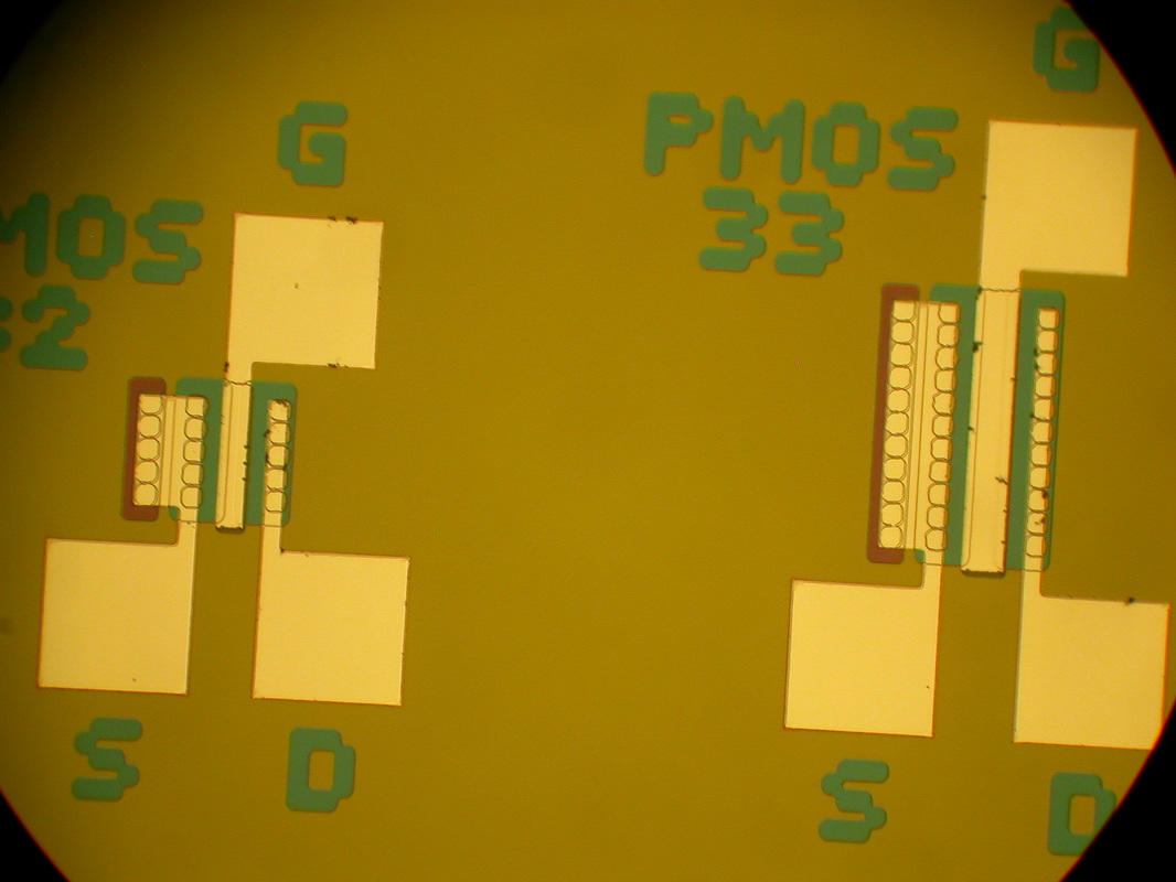
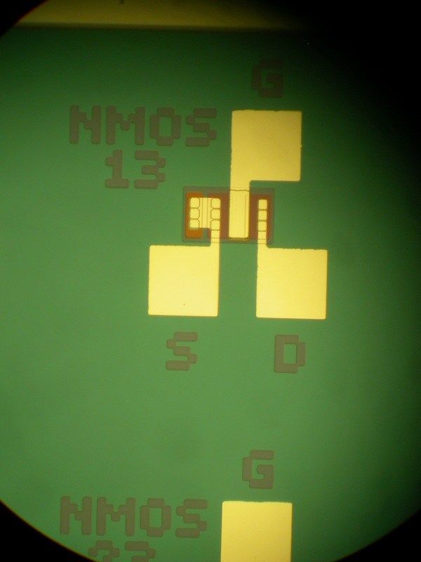
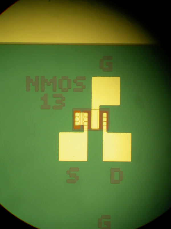
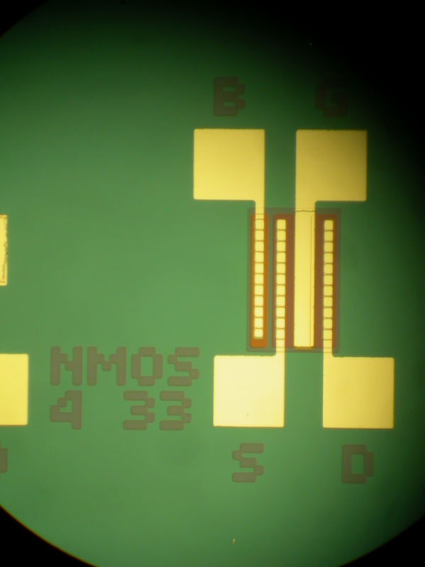
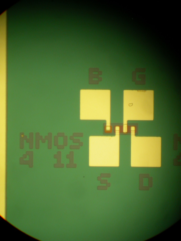
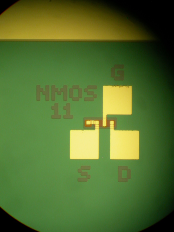
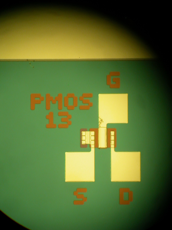
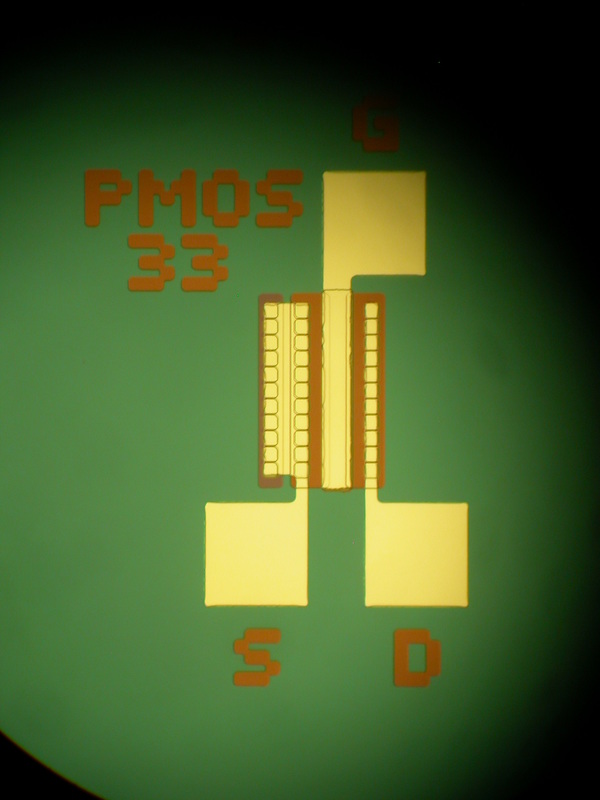
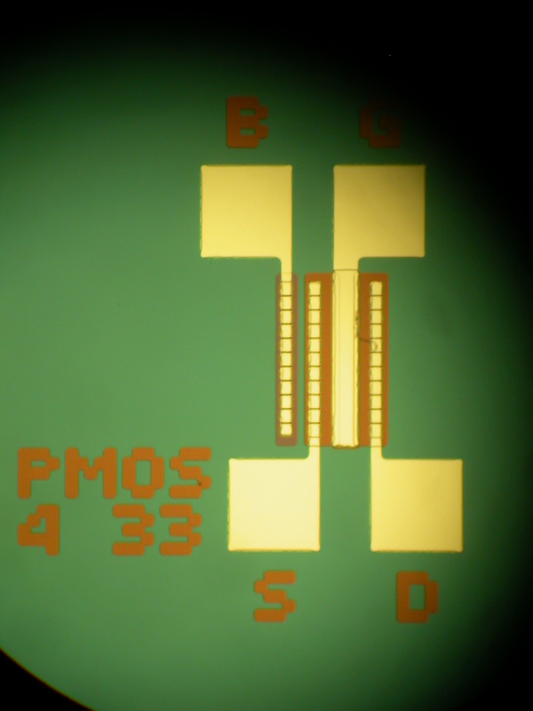
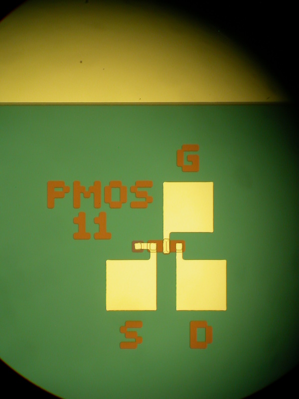
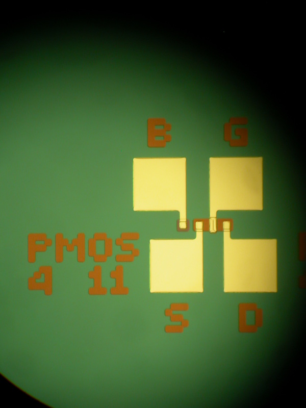
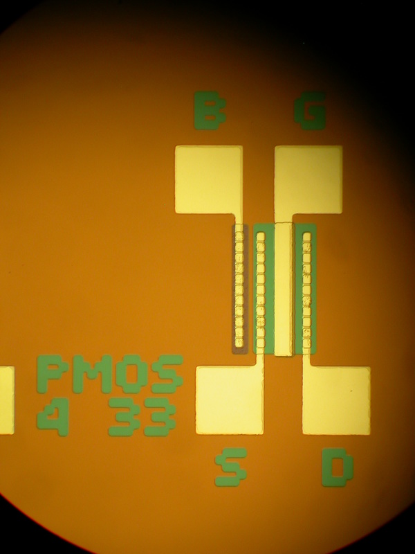
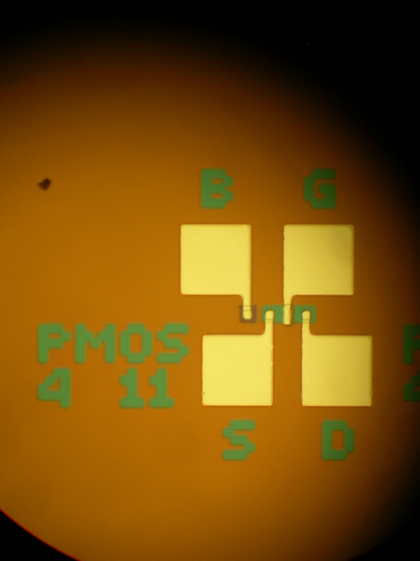
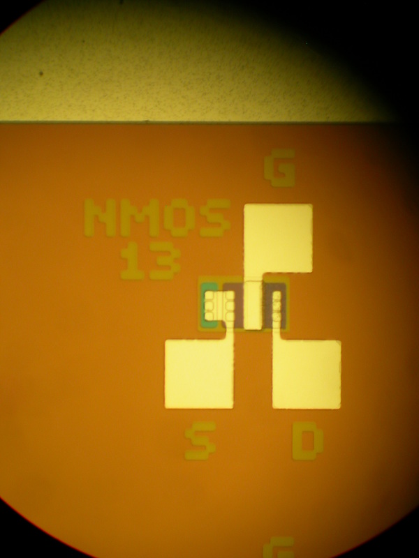
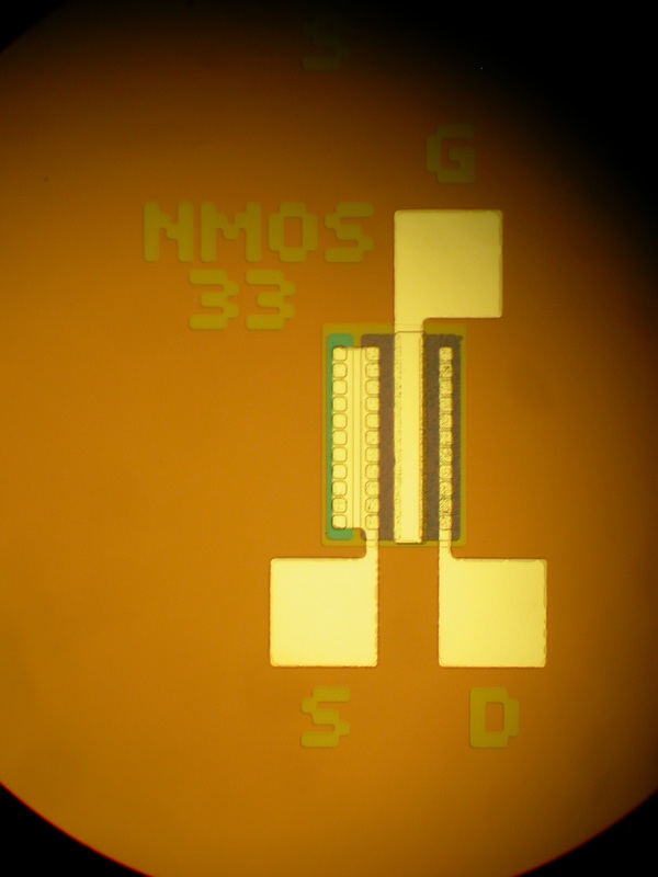
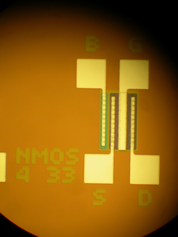
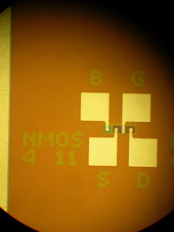
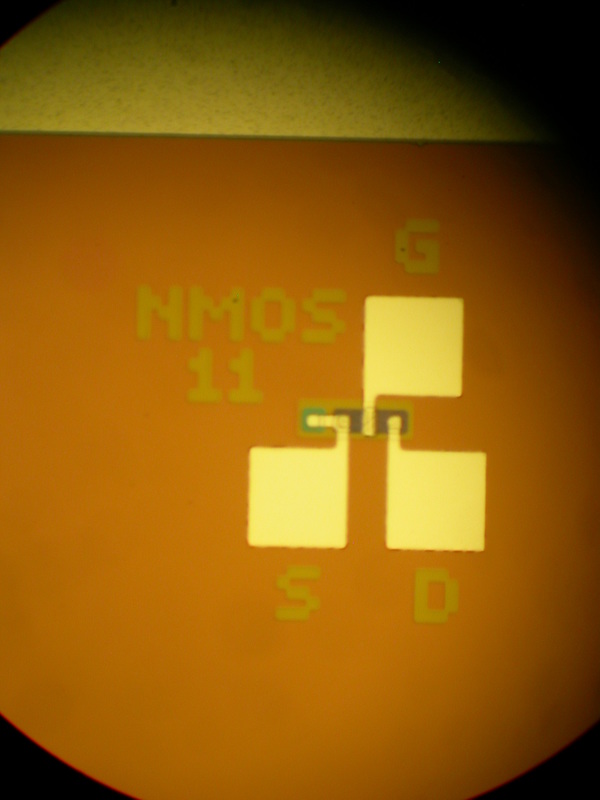
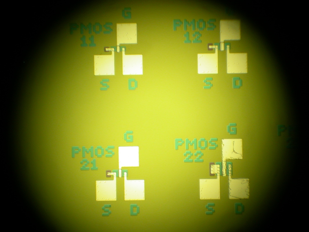
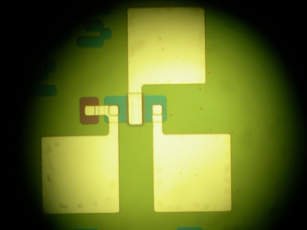
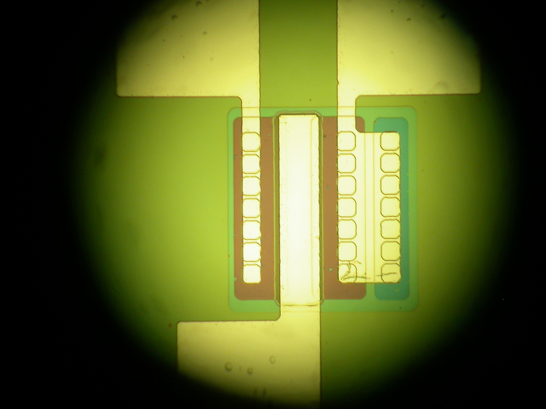
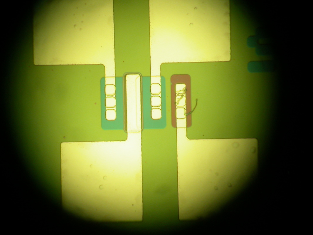
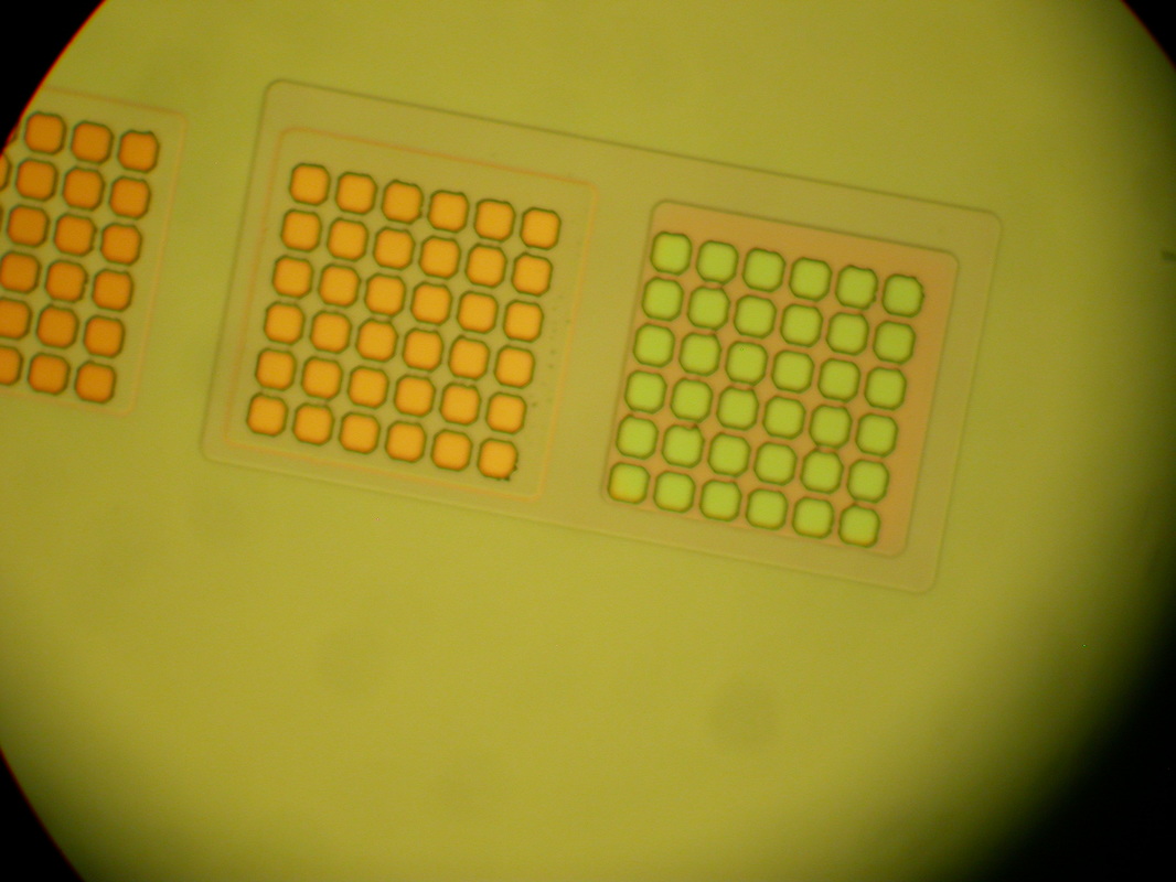
Images of completed devices


Testing
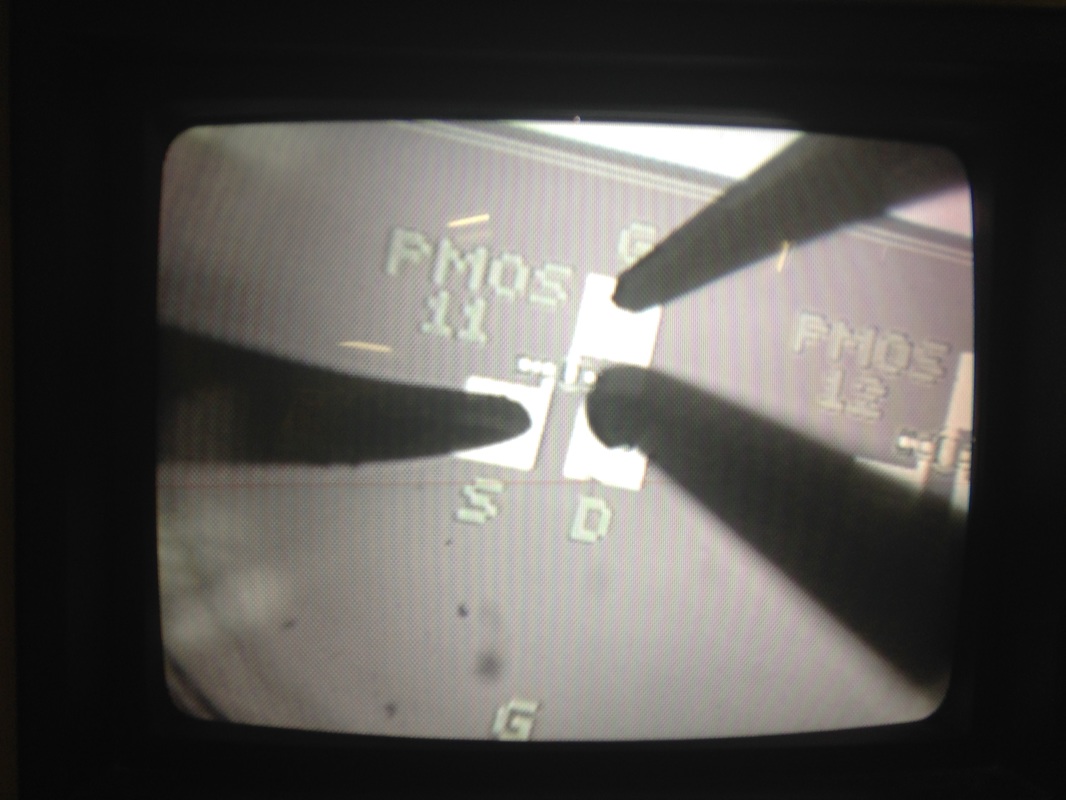
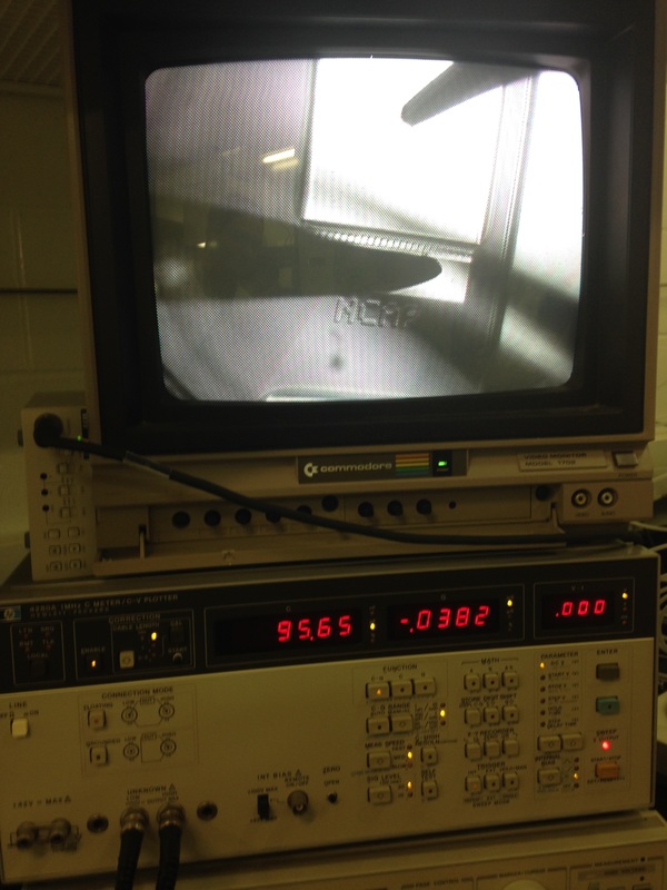
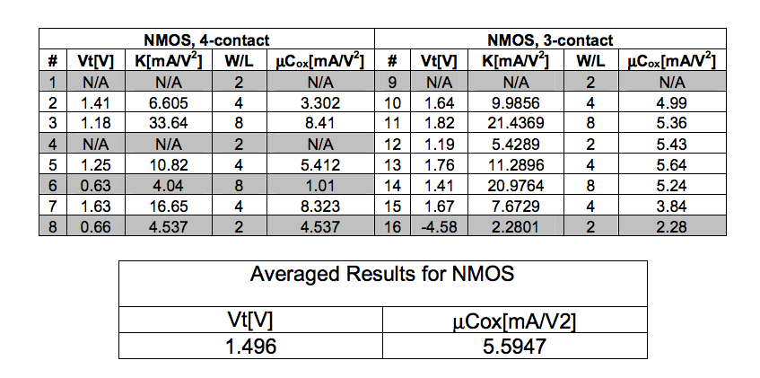
NMOS/PMOS Transistors

|
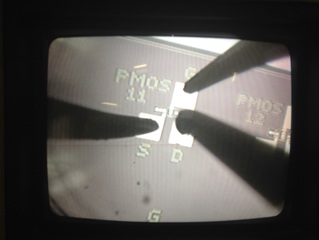
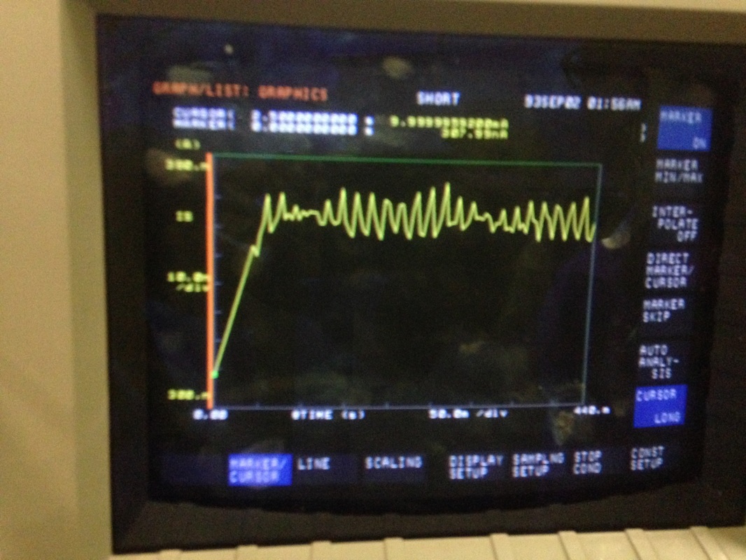
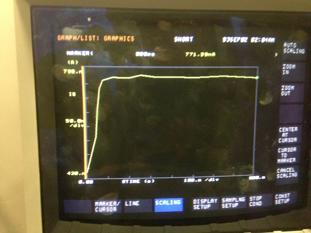
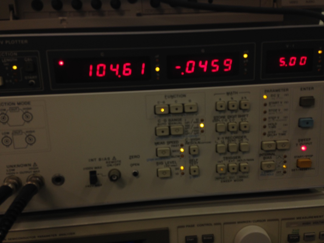
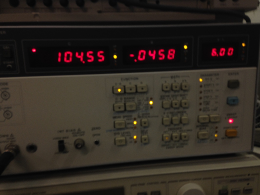
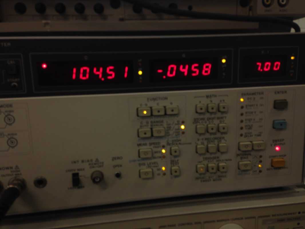
Three-probe device test machine monitor
|

|
NMOS

PMOS
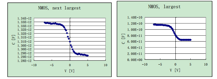
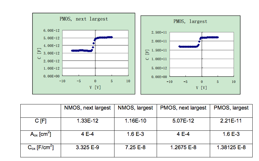
PMOS & NMOS Capacitors
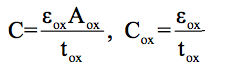
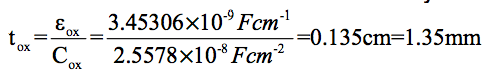
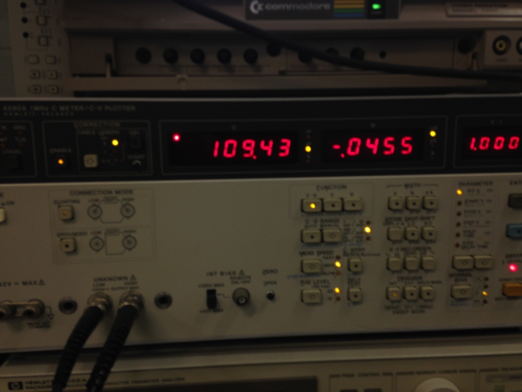
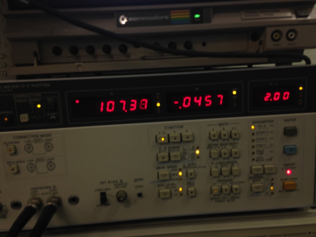
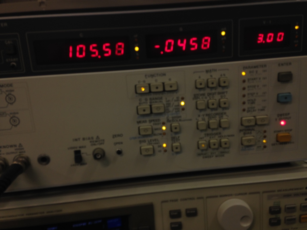
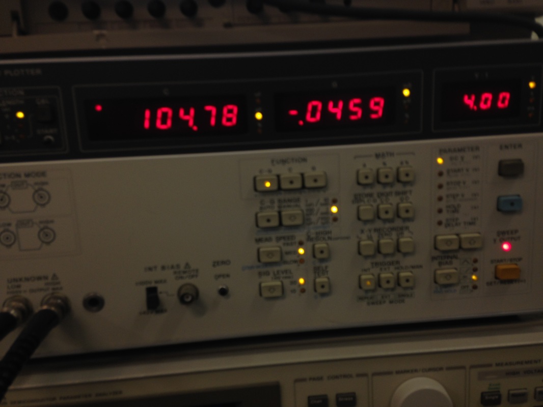
The averaged value of Cox is 2.5578×10⁻⁸ F/cm2 from the definition of capacitance above.The relative static permittivity (sometimes called the dielectric constant) εr of silicon dioxide is 3.9, and the electric constant ε0 is ~8.854×10⁻¹² F m–1. Then, we have εox=εrε0=3.45306×10⁻¹¹ F m–1.
|
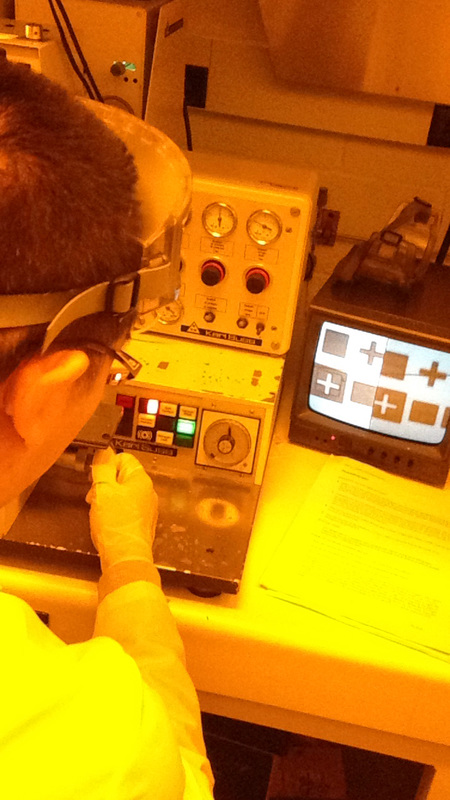
We used the C-V meter to measure the capacitance of the NMOS and PMOS capacitor structure. The bias voltages is given in the range of -7~5 V in .25 step. The oxide capacitance Cox is the maximum value measured. Note that Cox is measured in units of F/cm2.


|
Conclusions


Lab Documents
| equipment_manuals.zip |
| msds.zip |
| fab_sop.pdf |
| fab_cymos_traveler.pdf |
| fab_cymos_mask.pdf |
| fab_report1.pdf |
| fab_report2.pdf |
| fab_report_final.pdf |
